Materials Science: Unit IV: Optical Properties of Materials
Different electro optic modulators
These are used to modulate the intensity or phase of light by an electric field.
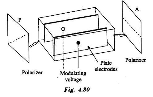
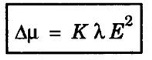
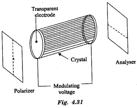
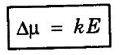
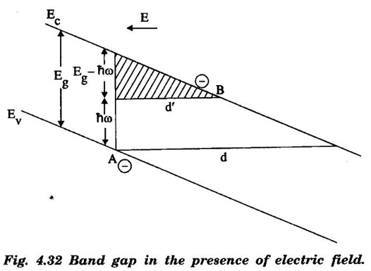
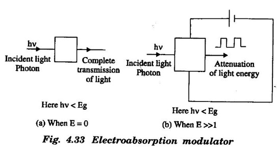
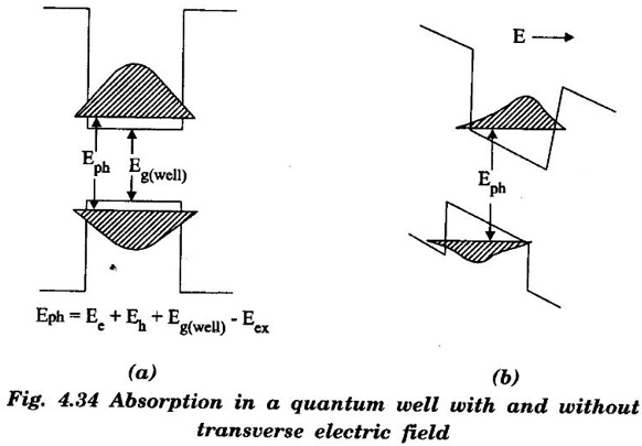
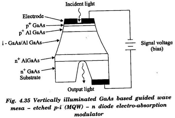
MODULATORS These are used to modulate the intensity or phase of light by an electric field. The different electro optic modulators are (a) Electrooptic modulators based on Kerr effect. (b) Electrooptic modulators based on Pockels effect. (c) Electro absorption modulator by Franz Keldysh and stark effect. (d) Quantum well electro absorption modulator. Optical anisotropy induced in an isotropic liquid under the influence of an electric field is known as the Kerr effect. (John Kerr discovered it in 1875). A Kerr cell is required for studying the effect. It consists of a sealed glass cell filled with a liquid comprising of asymmetric molecules. Two plane electrodes of length L are arranged parallel to each other. When a voltage is applied to the electrodes a uniform electric field is produced in the cell. The Kerr cell is placed between a crossed polarizer system. The molecules of the liquid tend to align along the electric field direction. (Fig. 4.30) As the molecules are asymmetric, the alignment causes anisotropy and the liquid becomes double refracting. The induced birefringence is proportional to the square of the applied electric field (E) and to the wavelength of incident light (λ). Thus Δμ ∝ λ Δμ ∝ E2 where K is known as the Kerr constant. The vibration direction of plane polarized light passing between crossed polarizer is rotated. Among the liquids, nitrobenzene (C6H5NO2) is found to have the highest value for the Kerr constant. therefore, Kerr cells use nitrobenzene. Kerr cell is used as (i) an electro-optic shutter in high-speed photography. (ii) a light chopper in the measurement of the speed of light. F. Pockels discovered in 1893 that the application of an electric field to piezoelectric crystals makes them birefringent. Normally, piezoelectric crystals are birefringent but in certain directions do not exhibit double refraction. When an electric field is applied along these directions, double refraction is induced along these directions also. A Pockels cell consists of a piezoelectric crystal, for example lithium niobate placed between crossed polarisers. Transparent electrodes (thin conducting coatings of tin oxide or indium) are deposited on opposite sides of the crystal. The crystal is oriented with its optic axis along the direction of the electric field. The transparent electrodes ensure free propagation of light through the crystal. A Pockels set up is shown in fig.4.31. The birefringence induced in the crystal is proportional to the strength of the applied field. Thus, Δμ ∝ E where k is a constant depends on characteristic of the material. Equ. shows that Pockels effect is a linear effect. The total birefringence of the cell is initially made equal to λ/2. When the electric field is increased, the beam is transmitted or hindered depending on the phase difference between the o-ray and e-ray. The device switches on and off periodically. Pockels cells are used in fast switching applications and in fibre optics. It can be used to obtain amplitude, frequency or phase modulation. The piezoelectric crystals of ammonium dihydrophosphate (ADP) and potassium dihydrophosphate (KDP) are widely used in Pockels cell. Kerr and Pockels cells are widely used as electro-optic shutters in Q-switching of lasers. Generally, semiconductors absorb the photon when the photon energy is equal to or greater than the bandgap energy (Eg) of the semiconductor. In some cases the doped impurities in the semiconductor may also absorb the photons. For this absorption, the energy of the photon must be at least equal to the ionization energy of the impurity atom. This low energy donor band and acceptor band absorption transitions have been observed in many semiconductors. The absorption of light photons having energies less than the band gap energy of the semiconductor by applying a strong electric field is called as Franz Keldysh effect. Fig. 4.32 shows the bending of energy bands due to the presence of electric field. When there is no photon and the electric field, the wave functions of electron at A (valance bond) and B (conduction band) are decaying without overlapping in the bandgap. The increase of electric field (E), decreases the distance AB and hence the overlapping of wave functions within the energy gap increases. When there is no photon, the valence electron has to tunnel through a triangular barrier of height 'Eg' and thickness d = Eg/qE. By absorption of photon having energy hv < Eg the thickness is reduced to Eg – hv / qE. Therefore the overlapping of the wavefunctions further increases and the electron from valence band can easily tunnel to the conduction band. Thus, an absorption of photon having energy hv < Eg in the presence of strong electric field produces electron tunneling. Thus the Franz-Keldysh effect is a photon assisted tunneling of electron through the barrier. The absorption of photon by the electron depends on the strength of applied field. Generally, the Franz Keldysh effect occurs when the applied electric field E is more than 107 V m-1. The Energy level splitting of the outer 2s or 2p states and hence absorption of photon whose energy is less than the band gap by an applied electric field is called Linear stark effect. Energy level splitting of ground level (1s) states and hence absorption of photon whose energy is less than the bandgap by an applied electric field is known as quadratic or second order stark effect. Thus the Franz - Keldysh effect and Stark effect refer to the electron tunneling via electro-absorption. Using these effects the modulation of light can be done by applying sequence of electric pusles. These type of modulators are called electroabsortion modulators. Consider the light photon energy smaller than the bandgap energy of semiconductor. When there is is no applied field (Fig.4.33), the light photon is completely transmitted without any absorption. When the bias pulses are applied which correspond to the signal to be transmitted, there is attenuation of transmitted light depending upon the value of magnitude of applied bias pulses. 1. The electroabsorption effects are very weak. 2. To increase the clectro absorption effect, very large electric fields (107 V/m) or very long devices (~ several millimetres) are needed. Hence these electroabsorption effects are not used to modulate the light since the applied field signal is not very large. The electron in a potential well of infinite depth cannot escape through the walls of the potential well. Thus, the electron is confined in the region defined by the well width. Further its energies are quantised. Figure 4.34 shows the ground sate wavefunctions of the electron and hole sub band with zero field. Taking Eph = absorbed photon energy, Ee and Eh are the electron an hole subband energies, Eex= binding energy of exciton and Eg (well) = bandgap energy between conduction band and valence band. The transition energy is given by finite transverse electric field (fig. 4.34(b)). When there is an applied transverse electric field (107 V/m), the bending of quantum well takes place. Further the electron and hole wavefunctions are pushed toward the opposite sides of the well. Eph = Ee + Eh + Eg(well) - Eex There is a little change in Eex and a very small change in Eg(well) due to stark effect in the well material. But due to the modification in the envelope of the wave functions of hole and electron, there is a reduction in Ee and Eh the subband energies. A quantum well is a potential well with thick walls (≈100Å). The electrons and holes (particles) are confined in the region defined by the well width. Similarly there is also multiple quantum well formed by two or more lattice matched materials. So the ground state inter-subband energy separation is very small. This results in a shift of the absorption spectrum to lower energies. This shift is the dominant effect which results a pronounced red shift of the absorption edge. This shift is called Quantum Confined Stark Effect (QCSE). This shift is larger than the stark shift (or) Franz - Keldysh effect in bulk semiconductors. This enormous shift is due to small size (100 Å) of quantum well. The shift is proportional to square of the electric field and to fourth power of the quantum well width. This effect is utilised to design efficient electroabsorption light modulators. When the energy of the incident photon is (20 meV) below the heavy hole exciton absorption (50 meV) at zero applied electric field, there is no absorption of the incident light. So the input light is completely transmitted through the quantum well material. When there is an applied transverse field of 107 V/m ((or) a transverse applied voltage of about 1 volt in the quantum well material) the heavy hole exciton absorption edge shifts and coincides with the photon energy. This results in strong absorption. Therefore there is an efficient intensity modulation of light. Construction working Fig. 4.35 shows the schematic diagram of p-i (MQW)-n diode quantum well electroabsorption modulator. It is mesa-etched GaAs modulator. The total thickness of Multi Quantum Well region is about 1 μm and the diameter of the mesa diode is about 50 to 100 μm. • The optical window (i.e. entrance gate for incident light) is situated at the top of the p-i-n diode is about half of the diode area. The p-i-n diode is made by photo lithography, selective selective etching and ohmic contact formation. • Since the GaAs substrate is not transparent to light, it is selectively etched under the active region of the diode. The light is transmitted through the diode or normal to the plane of the quantum well layers. • It is available in the form of integrated and waveguide form. Due to the waveguide structure and optical confinement, there is a single mode transmission. • Since the p-i-n diode is reverse biased, when there is no applied transverse electricfield, there is no flow of current in the external circuit. When there is an applied transverse fie (or bias signal), the incident light photon is absorbed and corresponding there is an increased current flow in the external circuit. Thus the modulation of light takes place which is proportional to the applied transverse electric field or bias signal strength. The modulation band width of 40 GHz can be obtained because of very small time constant of the device.KERR EFFECT
Pockels Effect
Franz - Keldysh and Stark Effect Electroabsorption Modulators
(i) Franz - Keldysh effect:
(ii) Stark effect:
Drawbacks
Quantum well electroabsorption modulators
p-i (MQW) - n diode quantum well electroabsorption modulator
Materials Science: Unit IV: Optical Properties of Materials : Tag: : - Different electro optic modulators
Related Topics
Related Subjects

Materials Science
PH3251 2nd semester Mechanical Dept | 2021 Regulation | 2nd Semester Mechanical Dept 2021 Regulation