Materials Science: Unit V: Nanoelectronic Devices
Resonant Tunneling
Definition, Explanation, Resonant Tunneling Diode
The phenomenon in which the tunneling current reaches peak (maximum) value
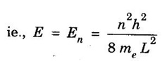
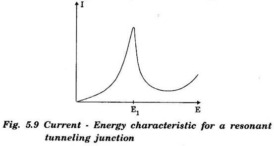
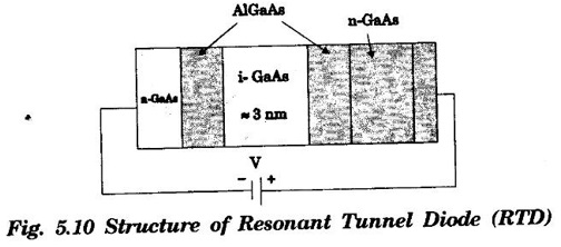
RESONANT TUNNELING The phenomenon in which the tunneling current reaches peak (maximum) value, when the energy of incident electron wave is equal to quantized energy state of the quantum well formed by the double symmetric barriers is known as resonant tunneling. An interesting phenomena occurs when two barriers of width a separated by a potential well of small distance L as shown in fig. 5.8. This leads to the concept of resonant tunneling. The barriers are sufficiently thin to allow tunneling and the well region between the two barriers is also sufficiently narrow to form discrete (quasi-bound) energy levels, as shown in fig. 5.8. The analysis of the double barrier structure is essentially the same as considered for single barrier tunneling. The transmission coefficient of the double symmetric barrier becomes unity (ie., T = 1), when the energy of the incoming electron wave (E) coincides with the energy of one of the discrete states formed by the well. where n = 1, 2, 3 ... Thus, transmission probability of the double symmetric barrier is maximum and hence, the tunneling current reaches peak value when energy of electron wave is equal to quantised energy state of the well. This phenomenon is known as resonance tunneling. The double barrier tunnel junction has important applications to a device known as a resonant tunneling diode. The working of these diodes can be understood considering the influence of bias on the energy band diagrams for the double barrier system. When the incident electron energy E is very different from the energy of a discrete state En, transmission is low. As E tends to En, transmission will increase, becoming a maximum when E = En. For example, assume that incident electrons have energy E, and that, all the energy states En lie above E, as shown in fig. 5.8. As E increases, tunneling will increase, reaching a peak when E = E1. After that point, a further increase in E will result in a decreasing current, as shown in fig. 5.9. This decrease of current with an increase of bias is called negative resistance. Further, peaks and valleys will occur as E approaches, and then moves across, other discrete energy states. A typical resonant tunneling diode structure is made by using n-type GaAs for the regions to the left and right of both barriers (regions 1 and 5) in fig. 5.10 intrinsic GaAs for the well region (region 3) and AlGaAs or AlAs for the barrier material (regions 2 and 4 in fig. 5.10). Tunneling is controlled by applying a bias voltage across the device.Definition
Explanation

Resonant Tunneling Diode (RTD)
Materials Science: Unit V: Nanoelectronic Devices : Tag: : Definition, Explanation, Resonant Tunneling Diode - Resonant Tunneling
Related Topics
Related Subjects

Materials Science
PH3251 2nd semester Mechanical Dept | 2021 Regulation | 2nd Semester Mechanical Dept 2021 Regulation