Materials Science: Unit V: Nanoelectronic Devices
Quantum structures (quantum wells, wires and dots)
Definition, Explanation, 3 types and its Construction, Use
When a bulk material is reduced in its size, atleast one of its dimension, in the order of few nanometres, then the structure is known as quantum structure.
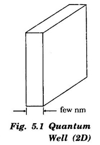
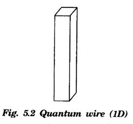
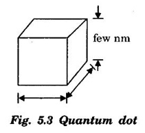
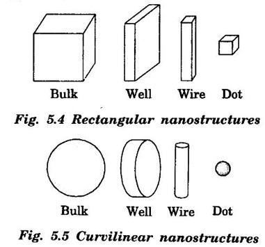
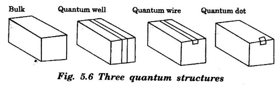
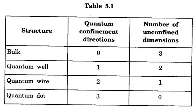
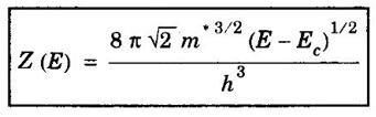
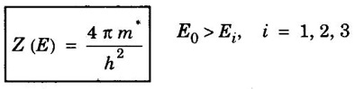
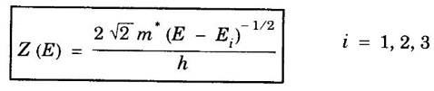
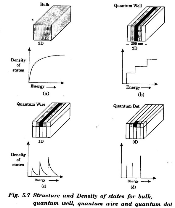
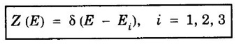
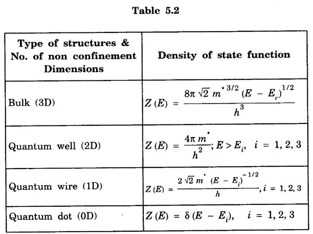
QUANTUM STRUCTURES (Quantum Wells, Wires and dots) When a bulk material is reduced in its size, atleast one of its dimension, in the order of few nanometres, then the structure is known as quantum structure. The volume of a box can be reduced by shortening its length, width or, and height. The same is true for the region occupied by the electrons in a solid. There are three dimensions to confine the bulk material. The quantum confinement needs confining at least one of these dimensions to less than 100 nanometres or even just a few nanometres. The more the dimensions are confined, the more the density of states function looks like that of an atom. This progressive discretization gives new ways to understand real atoms, behavior of electrons and developing quantum confined electronic devices. A structure in which the motion of the electrons or holes are confined in one or more directions by potential barriers is called quantum confined structure. The quantum confined structure is classified into three types based on the confinement directions. They are (i) quantum well (ii) quantum wire (iii) quantum dot Definition When the electrons are confined inside a region of minimal width ie., confinement in one dimension "quantum-well" is created. In other words, if one dimension is reduced to the nanometre range while the other two dimensions remain large, then we get a structure known as quantum well. Fig. 5.1 shows a quantum well or 2-D structure Construction Quantum wells are made from alternative layers of different semiconductors or by deposition of very thin metal films. Explanation The quantum well is a larger structure in which the carrier particles are free to move in two dimensions. The particles are confined in one dimension hence, they are considered to be quantum confinement. Due to the confinement of carriers, the quantum well structure has important applications in making useful devices. Use Quantum wells are now widely used to make semiconductor lasers and other important devices. Definition When the electrons are confined in two mutually perpendicular directions, then the structure is known as quantum wire. In other words, if two dimensions are reduced and one remains large, the resulting structure is quantum wire. Fig. 5.2 shows a quantum wire or 1-D structure Explanation The carriers trapped in such structures are considered to be in 1-D quantum confinement. In this case, a carrier is only free to move its trajectory along the wire. Example Examples of quantum wire structures are nanowires, nanorod and nanotube. Definition When all the three dimensions are minimized, the resulting structure is known as quantum dot. The dot can be particle located inside a larger structure or on its surface. It can also be a place where electrons have been trapped using electrical fields. Fig. 5.3 shows a quantum dot or 0-D structure Explanation In quantum dot, the carriers has only confined states i.e., there are no freely moving. Though a quantum dot has many thousands of atoms, carriers it is considered more like a single atom due to its peculiar properties. Use Quantum dot can be used in a quantum computer and quantum dot lasers etc. Fig. 5.4 and Fig. 5.5 explains the processes of diminishing the size in the case of rectilinear geometry and curvilinear geometry, respectively. Fig. 5.6 shows a comparison of three quantum confined structures with bulk material. As quantum wells and quantum wires each have at least one dimension in which the electrons are free to move and these structures exhibit "partial confinement". However, quantum dots exhibit "total confinement”. The classification of quantum confined structures is shown in Table 5.1. Density of states in Quantum Well, Quantum Wire and Quantum Dot Structure Bulk Structure The density of state of a bulk material is given by where Ec - bottom of conduction band energy m* - effective mass of electron The density of state curve is curve is parabolic as shown in fig. 5.7(a). Quantum Well Structure In quantum well structure, the electrons can move freely in two directions (2D) and confined in only one direction. The density of state of the quantum well structure The density of state function is constant and it gives step like function with energy as shown in fig. 5.7 (b). Quantum Wire Structure The quantum wire structure provides only one non confinement direction, ie., the carrier can move freely along one direction (1D). The remaining two directions are confined for charge carrier. The density of states of quantum wire is proportional to 1/√E. The density of state for this structure is given as The density of states function with energy is as shown in fig. 5.7(c). Quantum dot In a quantum dot all the directions are confined and no direction (OD) in which electron movement is free. The density of state for this structure is given by For quantum dot (OD) or nano particle, the permitted energy values are not continuous but form discrete bunches of varying densities. Thus, density of energy levels appear as discrete line as in fig. 5.7(d). Table 5.2 gives different quantum structures and their corresponding density of state functions.Definition
Explanation
(i) Quantum well (2 dimension)
(ii) Quantum wire (1 dimension)
(iii) Quantum Dots (0 - dimension)
Materials Science: Unit V: Nanoelectronic Devices : Tag: : Definition, Explanation, 3 types and its Construction, Use - Quantum structures (quantum wells, wires and dots)
Related Topics
Related Subjects
Materials Science
PH3251 2nd semester Mechanical Dept | 2021 Regulation | 2nd Semester Mechanical Dept 2021 Regulation