Materials Science: Unit V: Nanoelectronic Devices
3D photonic crystals
In a 3D photonic crystal, the dielectric constant is made to vary periodically in three dimensions.
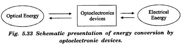
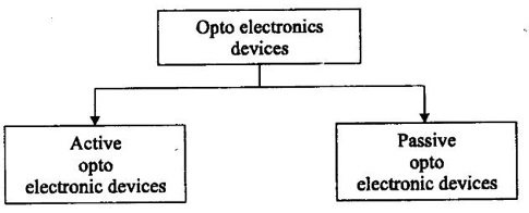
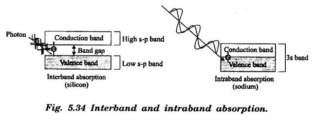
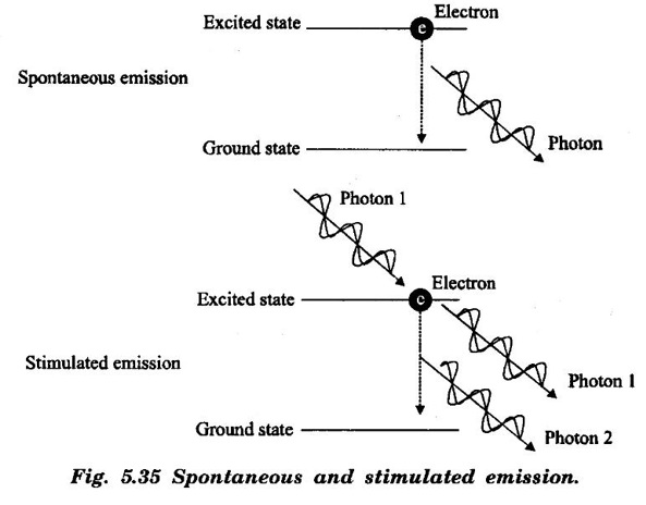
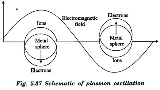
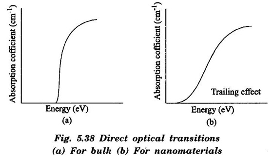
3D PHOTONIC CRYSTALS In a 3D photonic crystal, the dielectric constant is made to vary periodically in three dimensions. In this photonic crystal photonic bandgap prohibits electromagnetic propagation. It substantially modifies the dispersion around a specific wavelength (frequency) region. One of the greatest challenges in realizing 3D photonic crystals is the efficient fabrication of large-dimension (> 1000 unit cells) crystals with high refractive index variation. The large 3D periodic nanostructures can be produced by 1. Layer-by-layer photolithography 2. Colloidal self-assembly, 3. Direct laser writing, and 4. Holographic lithography. A schematic of 3D photonic crystal and its reflectivity for range wavelength is shown in fig. 5.32(b). The basic working process of optoelectronics deals with the optical interaction on the electronic responses in some specific optically active semiconducting materials. The semiconducting materials are preferred as the natural choice, due to the variation in their electrical conductivity over orders of magnitude by changing in temperature, optical excitation and the presence of impurity content in them. The devices which suport that type of interaction are known as optoelectronic devices. It is accompained by energy conversion from optical energy to electrical energy or vice versa, as shown in fig. 5.33 There are two types of optoelectronics devices. They are (i) Active optoelectronic devices. (ii) Passive optoelectronics devices In active optoelectronic devices, the light intensity can be directly varied in accordance with applied input voltage source the external light is not needed for its working. Example (i) Light Emitting Diode (LED) (ii) Laser diode (iii) Quantum well modulator (iv) Self electro optic effect switches In passive optoelectronics devices, the light intensity is not changed by controlling voltage. On the other hard, the plane of polarisation is turned by the application of control voltage. In passive optoelectronics devices, the external light source such as polariser and analyser are required. Examples (i) Kerr cell (ii) NLO crystals etc There are important processes. They are (i) Photon absorption (ii) Photon emission (iii) Photon scattering Photon absorption by insulators and semiconductors is likely to occur only if the photon's energy exceed that of the band gap. In figure 5.34, a photon of short wavelength (and hence high energy) is exciting an electron across the band gap separating the unfilled conduction band of silicon from the filled valence band. This is known as "interband" absorption. In conductors (like the metal sodium), there are numerous available energy states within the partially filled valence band, and valence electrons can also absorb lower-energy (longer-wavelength) photons. This is known This is known as intraband absorption. An excited electron can emit a photon on its own or when prompted by an incoming photon. Either way, the electron drops back to its ground state. In stimulated emission, the incoming photon 1 is not absorbed by the electron but continues on, in phase and in the same direction as the newly emitted photon 2. A third interaction between photons and matter is scattering. Scattering occurs when a photon changes direction after it strikes a bit of matter. This is usually a type of scattering called "elastic scattering" where no energy is exchanged between the photon and the matter. A photon strikes the left most particle and is scattered without any loss of energy toward the second particle, where it is again scattered. However, the second particle acquires a portion of the photon's energy, so the redirected photon ends up with a somewhat lower frequency (and therefore a longer wavelength, λ2 > λ1). Nanomaterials have attracted much attention due to their novel optical properties that are markedly different from bulk materials. The reason for this change in optical properties is due to the quantum confinement of electrons in nanomaterials and surface plasma resonance. Surface plasmon is the natural oscillation of electron gas inside the nanosphere. It can appear on the surface of bulk solids, thin films, and nanoparticles. On the surface of bulk solids, surface plasmons appear as a propagating wave parallel to the surface. When the nanosphere size is smaller than the wavelength of incident light, the frequency of surface plasmon becomes comparable to the frequency of radiation due to constructive interference. Then a resonance occurs and surface plasmon resonance (SPR) is generated (Fig. 5.37). Efficient energy and charge transfer in nanoscale dimension further contribute to the novel properties. Linear and nonlinear optical properties of the material can be finely tuned by controlling their dimension and surface chemistry. The optical properties of nanomaterials depend on their size, shape, surface characteristics, doping, and interaction with the surrounding environment or other nanostructures. A change in size of the CdSe semiconductor nanoparticles alters their optical properties. (A 2.3 nm CdSe emits blue light, whereas a 5.5 nm CdSe emits red light) A change in the size of metal nanoparticles causes some change in their optical properties. Quantum size effect is most significant in semiconductor nanoparticles. In semiconductors, the bandgap energy is of the order of a few electron volts. As the size of the particle increases, absorption shifts towards the shorter wavelength (blue shifts) indicates increase in the bandgap energy. The Semiconductor nanoparticles show luminescence when excited by electrons, photons, or electric field. Photoluminescence (fluorescence or phosphorescence) occurs when the external stimulus is due to photons. When luminescence is observed by the application of an electric field, it is termed electroluminescence. It can be tuned to the desired wavelength for nanomaterials as their bandgap can be tuned with particle size. Nanomaterials show high quantum efficiency for cathodoluminescence also, in which luminescence is produced by electrons of very high energy incident on materials. Finally, thermoluminescence is very strong for nanomaterials which have defect levels and larger number of surface atoms that can act as efficient electron/hole traps. Optical reflectance is defined by the fraction of incident light reflected from the surface of a material. Metals show high reflectance. It is due to the presence of a partially filled conduction band. Thus, absorption and reflection of photons take a continuum of energies from the infrared to visible, region. Semiconductors, on the other hand, show low absorption and reflectance in infrared range and increases drastically at the bandgap and increases further in the ultraviolet region. Direct optical transitions for bulk and nanomaterials are shown in fig. 5.38. Absorption edge of nanomaterials denotes trailing effect as compared to bulk due to variation in density of states, surface restructuring and a random distribution of impurities. There are some fascinating applications of the optical properties of nanomaterials in the areas of optical detectors, lasers, sensors, imaging, phosphors, displays, solar cells, photocatalysis, photoelectrochemistry, and biomedicine. Some of these applications are listed as follows. 1. Suitable for optoelectronic materials such as switches, amplifiers, gratings, splitters, isolators, lasers, and detectors 2. Widely used in polymers to increase their refractive index, which makes them suitable as optical components 3. Useful in preparing abrasion-resistant coatings whose optical clarity can be enhanced 4. Nanoparticles in castings improve shielding against electromagnetic fields in computers 5. LCDs and organic LEDs developed using nanomaterials show better resolution of images.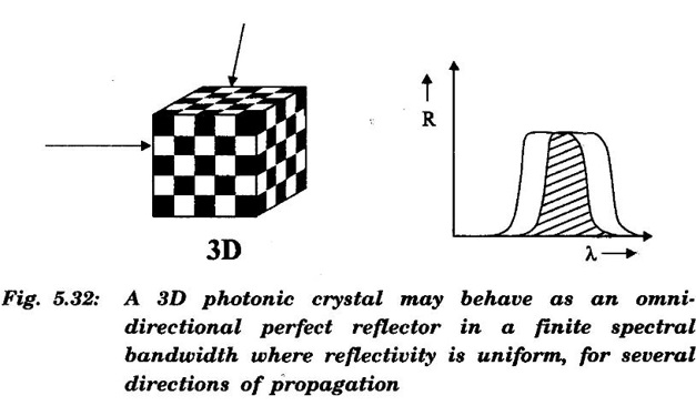
Optoelectronic Devices
Types of optoelectronics devices
Active optoelectronics devices
Passive optoelectronics devices
Difference between Active and Passive optoelectronics devices
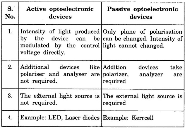
PHOTO PROCESS
Spontaneous and stimulated emission
Photon scattering
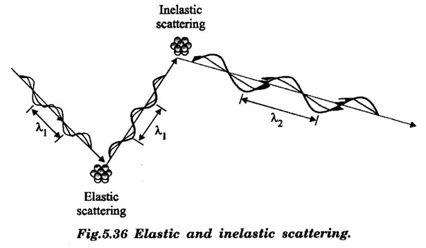
PHOTO PROCESS IN NANO STRUCTURES
Surface Plasmon
Other Factors that Contribute to Photon Properties
Quantum Size Effect
Luminescence
Optical Reflectance
Applications Based on Photo process
Materials Science: Unit V: Nanoelectronic Devices : Tag: : - 3D photonic crystals
Related Topics
Related Subjects
Materials Science
PH3251 2nd semester Mechanical Dept | 2021 Regulation | 2nd Semester Mechanical Dept 2021 Regulation