Basic Electrical and Electronics Engineering: Unit III: Analog Electronics
2 Marks Question & Answers
Analog Electronics | Basic Electrical and Electronics Engineering
2 Marks Question & Answers: Analog Electronics: Basic Electrical and Electronics Engineering
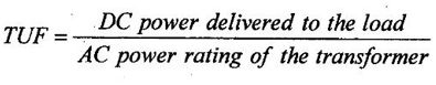
2 MARKS QUESTION & ANSWERS 1. What is semiconductor? Semiconductors are those substances which allow electric charges partially to flow through them. A semiconductor is a substance which has resistivity (10-4 to 0.5Ωm) in between conductors and insulators e.g. germanium, silicon, selenium, carbon etc. 2. What is meant by insulators? Insulators are those substances which do not allow electric current through them. Examples: Rubber, Wood, Glass etc., 3. What is meant by conductors? Conductors are substances which allow the flow of electric current through them. Examples: Copper, Aluminium, Salt solutions etc., 4. What is meant by Valence band? The energy band which possesses valence electrons is known as valence band. The electrons in the outermost orbit of an atom are known as valence electrons. The energy band possesses the valence electrons is called valence band. In a normal atom, valence band may be completely or partially filled. 5. What is meant by Conduction band? The energy band which possesses free electrons is known as conduction band. Electron in this band is responsible for conduction. 6. What is meant by Forbidden energy gap? There is a energy gap between conduction band and valence band on the energy level diagram is known as forbidden energy gap. 7. What is meant by intrinsic semiconductor? A pure form of Semiconductor is known as intrinsic semiconductor. Even at room temperature some of the valence electrons acquire sufficient energy to enter the conduction band to form free electrons. 8. What are extrinsic semiconductors? Adding impurities into the semiconductor materials (doping process) can control their conductivity. It is called impurity or extrinsic semiconductor. 9. What are p-type Semiconductor When a small amount of trivalent impurities such as Boron, Aluminium, gallium or Indium is added to a intrinsic semiconductor, it is known as p-type semiconductor. 10. What are n-type Semiconductor When a small amount of pentavalent impurities such as Arsenic, Phosphorous or Antimony is added to a intrinsic semiconductor, it is known as n-type semiconductor. 11. What are PN junction and draw it symbol. P-type Semiconductor and N-type Semiconductor are chemically combined with a special fabrication technique to form a PN Junction. 12. Define barrier potential. An electric field exists across the junction due to immobile positive and negative ions on opposite sides of the junction. This electric field is called as "barrier potential". 13. Define breakdown voltage. Under reverse biased condition, very small amount of reverse current (or) diode current will flow through a PN junction. While increasing the reverse bias voltage, a point may reach at which the junction breaks down which results in sudden rise in reverse current. The applied reverse bias voltage at which breakdown occurs with sudden rise in reverse current is called as breakdown voltage. 14. Define knee voltage. Under forward bias condition, forward current is very small till the applied voltage reach the barrier potential. The forward voltage, at which the forward current through the junction starts increasing rapidly is called as knee voltage (or) cut in voltage. 15. Define Peak inverse voltage. It is the maximum reverse voltage that can be applied to the PN junction without damage to the junction. If the reverse voltage exceeds its peak inverse voltage (PIV) the junction may get destroyed due to overheat. 16. Write Applications of PN junction diode. • Used as rectifiers • Used as switches • Used in power supply circuits • Used in clipper and clamper circuits 17. What is Diffusion or storage capacitance. The capacitance which exists in a forward - biased junction is called a diffusion or storage capacitance. It is called diffusion capacitance to account for the time delay in moving charges across the junction by diffusion process. 18. Depletion or Transition Capacitance When a PN-junction is formed, there exists a depletion region at the junction. this depletion region or layer consistes of positive and negative immobile ions. This depletion layer is non-conductive and hence acts as a dielectric medium between P-region and N- region. The P-region and N-region act as the two plates of a capacitor because they have a low resistance. These two plates are separated by a dielectric (depletion Layer). 19. What is zener diode and draw its symbol. In PN Junction diode, when the reverse bias voltage reaches breakdown voltage, the current through the junction increases and the power dissipated at the junction will be high. It causes the diode gets damaged. To avoid such a situation diodes can be designed with adequate power dissipation capabilities to operate in the breakdown region; such a diode is known as zener diode. Zener diodes are reverse biased heavily doped in junction diode. 20. What are beakdown mechanisms occurs in zener diode? The following two mechanism's cause junction breakdown due to the increase in reverse bias voltage. (i) Zener breakdown (ii) Avalanche breakdown 21. What are applications of Zener diode? (i) Used as voltage regulator. (ii) Used as peak clipper in wave shaping. (iii) Circuits used as fixed reference voltage in transistor biasing circuits. (iv) Used for protection meter against damage due to accidental application of over voltage. 22. What is rectifier? The process of converting ac voltage to pulsating dc voltage is known as rectification. A device which converts ac voltage to pulsating dc voltage is called as rectifier. 23. What are the types of Rectifiers? (i) Half-wave rectifiers. (ii) Full-wave rectifiers. 24. Define Transformer Utilization Factor (TUF). The TUF is defined as the ratio of dc power delivered to the load to the ac power rating of the transformer. 25. Define Load regulation. The load regulation is defined as the change in the regulated output voltage when the load current changes from minimum to maximum. Load regulation = VNL - VFL Where, VNL = load voltage with no load current VFL = load voltage with full load current Then, Percentage of Load regulation = 26. Define Line regulation. The line regulation is defined as the change in the regulated output voltage for specific range of line voltage. Line regulation = VHL- VLL Where, VHL = load voltage with high line voltage VLL = load voltage with low line voltage Percentage of line regulation = 27. What is Bipolar junction transistor? ● A Bipolar junction transistor is a three terminal semiconductor device which the operation depends on the interaction of majority and minority carriers. Hence it is named as Bipolar. ● Transistor is an abbreviation of transfer resistor is, signal transferred from low resistance circuit to high resistance circuit. 28. Define current amplification factor. The ratio of change in collector current to the change in emitter current at constant collector to base Voltage VCB is known as current amplification factor. 29. What are the operating regions in BJT? BJT can be operated in three regions: (i) Cut-off: In this region, both emitter-base and collector-base junctions are reverse biased. (ii) Active: In this region, the emitter-base junction is forward biased and the collector base junction is reverse biased. (iii) Saturation: In this region, both emitter-base and collector-base junctions are forward biased. 30. What are the three configurations of Transistor? There are three types of configurations for operation of transistor. They are, 1. Common base, 2. Common emitter, 3. Common collector 31. Define Early effect. ● The Early effect is the variation in the width of the base in a bipolar junction transistor (BJT) due to a variation in the applied collector to base voltage. ● When the VCB is made to increase, it increases the depletion region across collector to base junction, with the result that effective width of base decreases. This variation of effective base width by the collector to base voltage (VCB) is known as early effect (or) base width modulation. 32. Define Reach through or punch through. The collector current IC is independent of VCB over transistor operating range. However if VCB is increased beyond a certain value, IC increases rapidly because of avalanche effect. This condition is known as Reach through or punch through. When it occurs large current will flow, possibly destroying the device. 33. What is meant by biasing? To achieve faithful amplification, input circuit (i.e. base-emitter junction) of the transistor remains forward biased and output circuit (i.e. collector base junction) always remains reverse biased during all parts of the signal. It is called as transistor biasing. 34. What is the Need for biasing? The primary purpose of transistor biasing is to keep the base-emitter junction properly forward biased and collector-base junction properly reverse biased during the application of signal. It can be achieved with a bias battery or associating a circuit with a transistor. The circuit which provides transistor biasing is known as biasing circuit. The transistor biasing is very essential for the proper operation of transistor in linear region or active region. 35. What is meant by Q-Point or operating point? To operate the transistor in linear region, we should get a fixed dc collector current at a fixed dc collector voltage. These fixed values of dc collector current and dc collector voltage are expressed by a term called operating point or Quiescent point or Q-point. For faithful amplification, Q-point must be selected properly. 36. What is Field Effect Transistors? ● The FET is a three terminal semiconductor device in which the current flow through the conduction region is controlled by an electric field. ● FET is also known as Voltage controlled device, since the flow of current in the output side is controlled by Input voltage ● The operation of the FET depends on the majority carrier alone. So it is called Unipolar device. 37. What are the advantages of FET? ● Thermally more stable. ● It is immune to radiation. ● No offset voltage occurs. ● Due to its high input impedance, it is preferred for amplifiers. ● Less space is required and less noisy. 38. What are the classification of FET? FET is classified into two types. (i) Junction Field Effect Transistor (JFET) (ii) Metal Oxide Semiconductor Field Effect Semiconductor (MOSFET) 39. What is pinch off voltage? When the value of VGS is increased, the value of ID decrease and reaches zero at the voltage known as pinch off voltage VP (or) VGS(off) 40. Write the equation for Drain Current. Drain Current ID = IDSS = where IDSS = Saturation current; VGS = Gate to source voltage, VP= Pinch off voltage 41. What are the applications of JFET? (i) Since JFET is voltage controlled device, it is used as a voltage variable resistor in voltage control circuits, operation amplifiers etc. (ii) JFET can be used as an amplifier element in buffer amplifier, RF amplifier tuner circuit, operational amplifier etc. (iii) Due to its Voltage Variable Resistor function. It is used in an Automatic Gain Control Circuits. (iv) It is used as a mixer and oscillator in various frequency driven circuits. 42. Wwhat is Metal oxide Semiconductor FET? MOSFET is a three terminal semiconductor device. It is also known as Insulated Gate FET (IGFET) in which there is no pn junction structure, but instead the gate is insulated from the channel by oxide layer of SiO2 hence the name Insulated Gate FET. The electric field applied cross an insulated gate controls the majority carrier in the channel. 43. What are the Applications of MOSFET? (i) MOSFET is commonly preferred for implementing Logic gate. Hence it is widely used in switch, microprocessor, memory element etc. (ii) It is used as a discrete device in switch mode power supplies (SMPS), driven circuit etc. (iii) In the frequency driven circuit, it is used as a mixer and oscillator. (iv) It is used as a chopper amplifier and stabilization circuit in op-amp. (v) It functions as a switched capacitor circuits in time processing system. 44. What is IGBT? The IGBT or Insulated Gate Bipolar Transistor is the combination of BJT and MOSFET. It is a four-layer PNPN device having three PN junctions. It has three terminals Gate (G), Collector(C) and Emitter (E). The terminal's name also implies being taken from both transistors. Gate terminal as it is the input part, taken from MOSFET while the collector and emitter as they are the output, taken from the BJT. 45. What are the applications of IGBT IGBTs have numerous applications used in AC as well as DC circuits. Here are some of the important applications of IGBT ● It is used in SMPS (Switched Mode Power Supply) to supply power to sensitive medical equipment and computers. ● It is used in UPS (Uninterruptible Power Supply) system. ● It is used in AC and DC motor drives offering speed control. ● It is used in chopper and inverters. ● It is used in solar inverters. 46. What is SCR? Silicon Controlled Rectifier (SCR) is one of the oldest type of solid state power device. SCRS have the highest power handling capacity of all the power semiconductor devices. They have a four layer construction with three user accessible terminals. SCR is a latching type device that can be turned on by the control terminal (gate) but once turned on the gate loses control on it (i.e. it cannot be turned by the gate) 47. What is forward blocking state in SCR? This is the high voltage low current mode of operation in which SCR is in the OFF state. The current through it is Forward Leakage Current. This current flow due to thermally generated minority carriers. 48. What is inverter? An inverter is a device that change dc power into ac power (just the opposite of converters). The inversion process can be achieved with the help of transistors, SCRS and tunnel diodes etc.


Basic Electrical and Electronics Engineering: Unit III: Analog Electronics : Tag: : Analog Electronics | Basic Electrical and Electronics Engineering - 2 Marks Question & Answers
Related Topics
Related Subjects

Basic Electrical and Electronics Engineering
BE3251 2nd semester Mechanical Dept | 2021 Regulation | 2nd Semester Mechanical Dept 2021 Regulation

Basic Electrical and Electronics Engineering
BE3251 2nd Semester CSE Dept 2021 | Regulation | 2nd Semester CSE Dept 2021 Regulation