Basic Electrical and Electronics Engineering: Unit III: Analog Electronics
Zener Diode
Symbol, Biasing, VI Characteristics, Applications
In PN Junction diode, when the reverse bias voltage reaches breakdown voltage, the current through the junction increases and the power dissipated at the junction will be high.
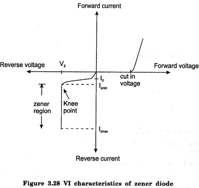
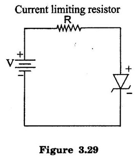
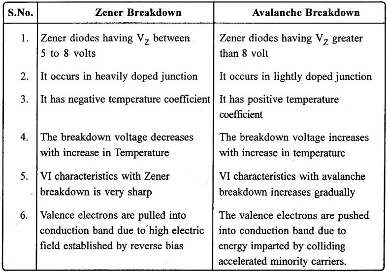
ZENER DIODE In PN Junction diode, when the reverse bias voltage reaches breakdown voltage, the current through the junction increases and the power dissipated at the junction will be high. It causes the diode gets damaged. To avoid such a situation diodes can be designed with adequate power dissipation capabilities to operate in the breakdown region; such a diode is known as zener diode. Zener is a reverse biased heavily doped PN junction diode which operates in the breakdown region. The breakdown voltage of zener diode can be set by controlling the doping level. If the diode is heavily doped, the depletion region will be narrow and consquently, breakdown occurs at lower reverse voltage and further, the breakdown voltage is sharp. 1. Forward characteristics: The forward characteristics of zener diode is shown in figure 3.28. Under forward biased condition, the operation of zener diode is same as that of ordinary PN diode. 2. Reverse Characteristics: When we increase the reverse voltage initially a small reverse saturation current I0(μA)will flow. This current flows due to the thermally generated minority carriers. At a certain value of reverse voltage, the reverse saturation current will increase suddenly and sharply. This indicates breakdown of the junction has occurred. This breakdown voltage is called as Zener breakdown voltage (or) Zener voltage (VZ). This breakdown voltage depends upon the amount of doping. After breakdown has occurred, the voltage across zener diode remains constant equal to VZ and reverse Zener current increased. The Zener current after reverse breakdown must be controlled by connecting resistor R as shown in figure 3.29 to avoid any damage to the device due to excessive heating. The following two mechanisms cause junction breakdown due to the increase in reverse bias voltage. (i) Zener breakdown (ii) Avalanche breakdown Let us understand the zener breakdown mechanism for zener voltage (VZ) less than 5V. If a reverse voltage (5V) is applied to a zener diode, it causes a very intense electric field (order of 3 × 10⁵V/cm) to appear across a narrow depletion region. This intense electric field is strong enough to pull some of valence electrons into the conduction band by breaking their covalent bonds. These electrons are now ready for conduction. A large amount of these electrons will constitute the large reverse current through the zener diode and breakdown is said to have occurred due to zener effect. The current limiting resistor is connected in series with zener diode to avoid damage due to excessive heating. The breakdown voltage depends upon the temperature of PN junction. The breakdown voltage decreases with increase in the junction temperature. As reverse voltage applied to the zener diode increases (>8V), the field across the junction increases correspondingly. An increase in reverse voltage, the minority carriers tends to accelerate. Hence kinetic energy associated with them increases. While travelling, these accelerated minority carriers will collide with immobile ions and create new electron hole pairs. These new carriers again acquire sufficient energy from the field and collide with other immobile ions or atoms. Due to this, further electron-hole pairs generated. This process is cumulative in nature. In short time the generation of avalanche of charge carriers available for conduction and carrier multiplication process becomes self sustained. This mechanism of carrier generation is known is "avalanche multiplication” (or) “avalanche effect". Hence, a large amount of reverse current flowing through the zener diode and the avalanche breakdown is said to have occurred. Applications of Zener diode: (i) Used as voltage regulator. (ii) Used as peak clipper in wave shaping. (iii) Circuits used as fixed reference voltage in transistor biasing circuits. (iv) Used for protection meter against damage due to accidental application of over voltage.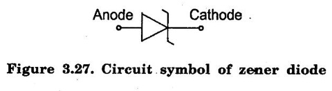
1. V.I. Characteristics of Zener diode:
2. Breakdown Mechanism
1. Zener breakdown
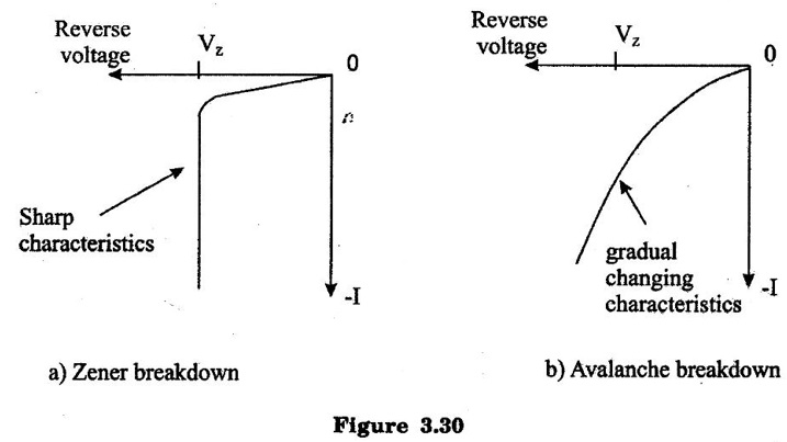
2. Avalanche breakdown
3. Comparison of Zener breakdown & avalanche breakdown.
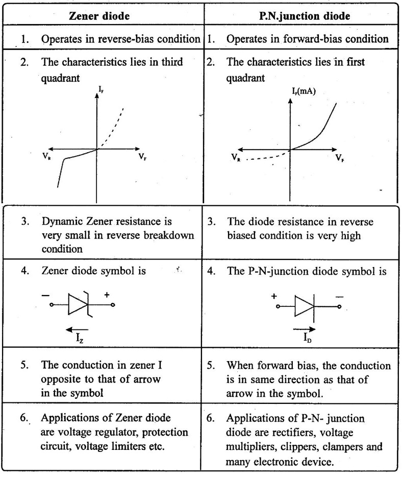
4. Comparison of Zener Diode and P-N Junction Diode
Basic Electrical and Electronics Engineering: Unit III: Analog Electronics : Tag: : Symbol, Biasing, VI Characteristics, Applications - Zener Diode
Basic Electrical and Electronics Engineering: Unit III: Analog Electronics
Under Subject

Basic Electrical and Electronics Engineering
BE3251 2nd semester Mechanical Dept | 2021 Regulation | 2nd Semester Mechanical Dept 2021 Regulation

Basic Electrical and Electronics Engineering
BE3251 2nd Semester CSE Dept 2021 | Regulation | 2nd Semester CSE Dept 2021 Regulation
Related Subjects

Professional English II
HS3251 2nd Semester 2021 Regulation | 2nd Semester Common to all Dept 2021 Regulation

Statistics and Numerical Methods
MA3251 2nd Semester 2021 Regulation M2 Engineering Mathematics 2 | 2nd Semester Common to all Dept 2021 Regulation

Engineering Graphics
GE3251 eg 2nd semester | 2021 Regulation | 2nd Semester Common to all Dept 2021 Regulation

Physics for Electrical Engineering
PH3202 2nd Semester 2021 Regulation | 2nd Semester EEE Dept 2021 Regulation

Basic Civil and Mechanical Engineering
BE3255 2nd Semester 2021 Regulation | 2nd Semester EEE Dept 2021 Regulation
Electric Circuit Analysis
EE3251 2nd Semester 2021 Regulation | 2nd Semester EEE Dept 2021 Regulation

Physics for Electronics Engineering
PH3254 - Physics II - 2nd Semester - ECE Department - 2021 Regulation | 2nd Semester ECE Dept 2021 Regulation

Electrical and Instrumentation Engineering
BE3254 - 2nd Semester - ECE Dept - 2021 Regulation | 2nd Semester ECE Dept 2021 Regulation
Circuit Analysis
EC3251 - 2nd Semester - ECE Dept - 2021 Regulation | 2nd Semester ECE Dept 2021 Regulation

Materials Science
PH3251 2nd semester Mechanical Dept | 2021 Regulation | 2nd Semester Mechanical Dept 2021 Regulation
Basic Electrical and Electronics Engineering
BE3251 2nd semester Mechanical Dept | 2021 Regulation | 2nd Semester Mechanical Dept 2021 Regulation

Physics for Civil Engineering
PH3201 2021 Regulation | 2nd Semester Civil Dept 2021 Regulation
Basic Electrical, Electronics and Instrumentation Engineering
BE3252 2021 Regulation | 2nd Semester Civil Dept 2021 Regulation

Physics for Information Science
PH3256 2nd Semester CSE Dept | 2021 Regulation | 2nd Semester CSE Dept 2021 Regulation
Basic Electrical and Electronics Engineering
BE3251 2nd Semester CSE Dept 2021 | Regulation | 2nd Semester CSE Dept 2021 Regulation

Programming in C
CS3251 2nd Semester CSE Dept 2021 | Regulation | 2nd Semester CSE Dept 2021 Regulation