Basic Electrical and Electronics Engineering: Unit III: Analog Electronics
Bipolar Junction Transistors
BJT Symbol, Biasing, VI Characteristics, Operational Principle
A Bipolar junction transistor is a three terminal semiconductor device in which the operation depends on the interaction of majority and minority carriers.
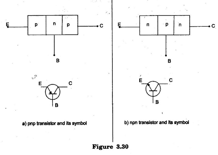
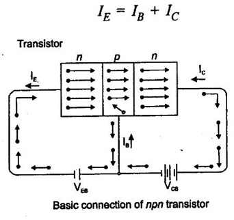
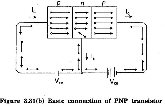
BIPOLAR JUNCTION TRANSISTORS ❖ A Bipolar junction transistor is a three terminal semiconductor device in which the operation depends on the interaction of majority and minority carriers. Hence it is named as Bipolar device. ❖ Transistor is an abbreviation of transfer resistor i.e., signal transferred from low resistance circuit to high resistance circuit. ❖ A transistor consists of a silicon or germanium crystal in which a layer of N-Type material is sandwiched between two layers of P Type material. It is referred to an PNP transistor. It is shown in figure 3.30(a). Alternatively, layer of P-Type material is sandwiched between two layers of N type material. It is referred to NPN transistor. It is shown in figure 3.30(b). ❖ There are three terminals in the transistor Emitter(E), Base(B), Collector(C). (i) Emitter: It is more heavily doped region than other two regions. The emitter is always forward biased with respect to base, hence it can supply majority carriers to the base. In case of PNP transistor, it supplies hole charges to its junction. In case of NPN transistor, it supplies free electrons with the base. (ii) Collector: Its main function is to collect the majority charge carriers from the emitter through base. In most of the transistors, the collector region is made physically larger than emitter region since it has to dissipate much greater power. (iii) Base: It is the middle section of the transistor. It is highly doped region. It is very thin as compared to either the Emitter or Collector. The emitter-base junction of a transistor is forward biased whereas collector- base junction is reverse biased. If the emitter-base junction is forward biased, the emitter current will flow to base region from emitter region. It is seen that this emitter current almost entirely flows in the collector circuit. Hence, the current present in the collector circuit depends upon the emitter current. If the emitter current is zero, then collector current is nearly zero [a very little current (few μA) would flow]. For example, if the emitter current is 0.5mA, then collector current is also around 0.5mA. (i) Working of npn transistor. ● Fig. 3.21(a) shows the charge carrier movement in a NPN transistor. Forward bias is applied to emitter-base junction and reverse bias is applied to collector-base junction of the npn transistor. Due to the forward bias, the electrons in the n-type emitter flow towards the base. It constitutes the emitter current IE. Since these electrons cross into p-type base, they tend to combine with the holes. ● As the p-type base is lightly doped and very thin, only few holes are present. Therefore, only few electrons from n-type emitter combine wish holes. It constitutes base current IB. The remaining electrons (more than 95%) cross into the collector region to constitute collector current IC. In this way, almost the whole emitter current flows in the collector circuit. From the above discussion it is concluded that the emitter current is the sum of collector and base currents i.e. (ii) Working of pnp transistor. ● Fig. 3.31(b) shows the charge carrier movement in a PNP transistor. The PNP transistor behaves exactly as same way as an NPN transistor except that the majority charge carriers are holes. Due to the forward bias, the holes in the p-type emitter flow towards the base. It constitutes the emitter current IE. Since these holes cross into n-type base, they tend to combine with the electrons. ● As the n-type base is lightly doped and very thin, only few electrons are present. Therefore, only a few holes (less than 5%) from p-type emitter combine with these electrons. It constitutes base current IB. The remaining holes (more than 95%) cross into the collector region to constitute collector current IC. In this way, almost the entire emitter current flows in the collector circuit. It may be noted that current conduction within pnp transistor due to flow of holes. However, in the external connecting wires, the current flow is still by electrons. ❖ Due to forward bias, the input circuit (i.e. emitter-base junction) has low resistance Whereas output circuit (i.e. collector-base junction) has high resistance due to reverse bias. ❖ From the above discussion, the input emitter current almost entirely flows in the collector circuit. Hence, a transistor transfers the input signal current from a low- resistance circuit to a high-resistance circuit. This is the key factor for the amplification characteristics of the transistor. It is the ratio of output current to input current. The ratio of change in collector current to the change in emitter current at constant collector to base Voltage VCB is known as current amplification factor. There are two types of basic transistor : 1. Bipolar Junction Transistor (BJT) 2. Field Effect Transistor (FET). BJT can be operated in three regions: (i) Cut-off: In this region, both emitter-base and collector-base junctions are reverse biased. (ii) Active: In this region, the emitter-base junction is forward biased and the collector base junction is reverse biased. (iii) Saturation: In this region, both emitter-base and collector-base junctions are forward biased.1. Introduction:
2. Working of Transistor
Importance of transistor action.
Current amplification factor (α).

Types of basic transistor:
Basic Electrical and Electronics Engineering: Unit III: Analog Electronics : Tag: : BJT Symbol, Biasing, VI Characteristics, Operational Principle - Bipolar Junction Transistors
Basic Electrical and Electronics Engineering: Unit III: Analog Electronics
Under Subject

Basic Electrical and Electronics Engineering
BE3251 2nd semester Mechanical Dept | 2021 Regulation | 2nd Semester Mechanical Dept 2021 Regulation

Basic Electrical and Electronics Engineering
BE3251 2nd Semester CSE Dept 2021 | Regulation | 2nd Semester CSE Dept 2021 Regulation
Related Subjects

Professional English II
HS3251 2nd Semester 2021 Regulation | 2nd Semester Common to all Dept 2021 Regulation
Statistics and Numerical Methods
MA3251 2nd Semester 2021 Regulation M2 Engineering Mathematics 2 | 2nd Semester Common to all Dept 2021 Regulation

Engineering Graphics
GE3251 eg 2nd semester | 2021 Regulation | 2nd Semester Common to all Dept 2021 Regulation
Physics for Electrical Engineering
PH3202 2nd Semester 2021 Regulation | 2nd Semester EEE Dept 2021 Regulation
Basic Civil and Mechanical Engineering
BE3255 2nd Semester 2021 Regulation | 2nd Semester EEE Dept 2021 Regulation
Electric Circuit Analysis
EE3251 2nd Semester 2021 Regulation | 2nd Semester EEE Dept 2021 Regulation

Physics for Electronics Engineering
PH3254 - Physics II - 2nd Semester - ECE Department - 2021 Regulation | 2nd Semester ECE Dept 2021 Regulation
Electrical and Instrumentation Engineering
BE3254 - 2nd Semester - ECE Dept - 2021 Regulation | 2nd Semester ECE Dept 2021 Regulation
Circuit Analysis
EC3251 - 2nd Semester - ECE Dept - 2021 Regulation | 2nd Semester ECE Dept 2021 Regulation
Materials Science
PH3251 2nd semester Mechanical Dept | 2021 Regulation | 2nd Semester Mechanical Dept 2021 Regulation
Basic Electrical and Electronics Engineering
BE3251 2nd semester Mechanical Dept | 2021 Regulation | 2nd Semester Mechanical Dept 2021 Regulation

Physics for Civil Engineering
PH3201 2021 Regulation | 2nd Semester Civil Dept 2021 Regulation
Basic Electrical, Electronics and Instrumentation Engineering
BE3252 2021 Regulation | 2nd Semester Civil Dept 2021 Regulation
Physics for Information Science
PH3256 2nd Semester CSE Dept | 2021 Regulation | 2nd Semester CSE Dept 2021 Regulation
Basic Electrical and Electronics Engineering
BE3251 2nd Semester CSE Dept 2021 | Regulation | 2nd Semester CSE Dept 2021 Regulation

Programming in C
CS3251 2nd Semester CSE Dept 2021 | Regulation | 2nd Semester CSE Dept 2021 Regulation