Basic Electrical and Electronics Engineering: Unit III: Analog Electronics
Transistor Configurations
Three types, Operation, Characteristics, Circuit diagram | Bipolar Junction Transistors (BJT)
A transistor is a three terminal device (Emitter, Base and Collector). However, when a transistor is to be connected with a circuit, we require four terminals; two for the input and two for the output.
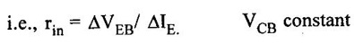
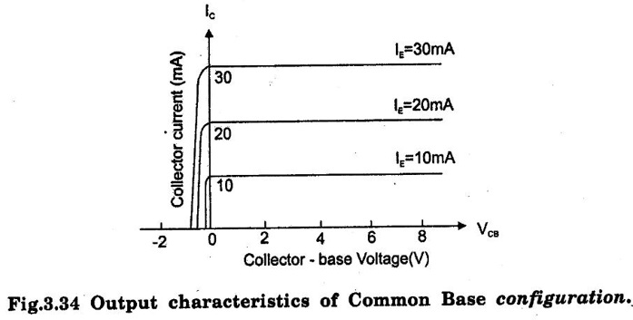
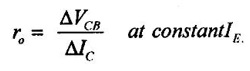
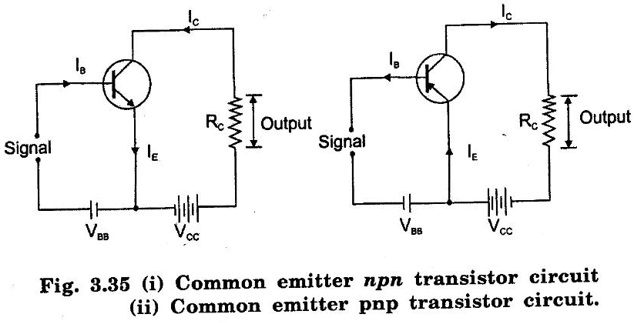
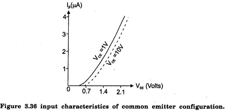
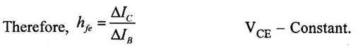
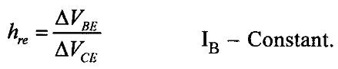
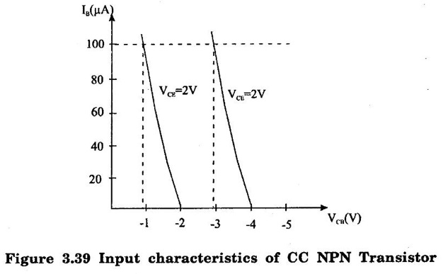
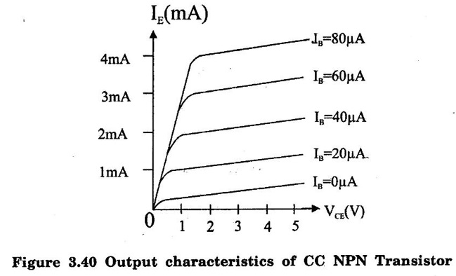
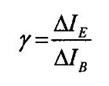
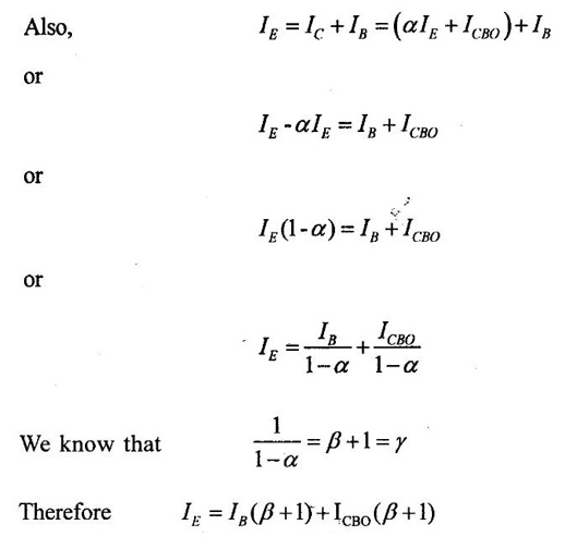
TRANSISTOR CONFIGURATIONS A transistor is a three terminal device (Emitter, Base and Collector). However, when a transistor is to be connected with a circuit, we require four terminals; two for the input and two for the output. This problem is overcome by making one of the terminal of the transistor common to both input and output terminals. There are three types of configurations for operation of transistor. They are, (i) Common base (ii) Common emitter (iii) Common collector Each configuration has its own advantages and disadvantages. It is to be noted that regardless of circuit configuration, the emitter is always forward biased, while the collector always reverse biased. ❖ In common base configuration, input is applied between emitter and base and output is taken across collector and base. Here, base is common to both input and output circuits and hence the name common base configuration. In Fig. 3.32(i), a common base npn transistor circuit is shown whereas Fig.3.32(ii) shows the common base pnp transistor circuit. ❖ In this arrangement, the emitter base junction is forward biased and collector base junction is reverse biased. The emitter current IE flows in the input circuit and the collector current IC in the output circuit. ❖ A change in the emitter current produces a change in collector current due to diffusion of electrons or holes across the junctions. The most important characteristics of common base configuration are input characteristics and output characteristics. 1. Input characteristics: ● Figure 3.33 Input characteristics of Common Base configuration. ❖ Figure 3.33 shows the input characteristics of a typical transistor in Common Base configuration. For determination of input characteristics, the collector-base voltage VCB is maintained constant and emitter-base voltage VEB varies to different levels. For each level of input voltage, the input current IE is noted. Then the curve is The emitter plotted between emitter current IE and emitter-base voltage VEB. The emitter current is taken along y-axis and emitter-base voltage taken along x-axis. (i) The emitter current IE increases rapidly with small increase in emitter-base voltage VEB. It means low dynamic input resistance because input resistance of a transistor is given as the reciprocal of the slope of its input characteristic. (ii) The emitter current is does not dependent of collector-base voltage VCB. leads to the conclusion that emitter current and collector current are almost independent of collector voltage. Input resistance: It is the ratio of change in emitter-base voltage (ΔVEB) to the resulting change in emitter current (ΔIE) at constant collector-base voltage (VCB) i.e. Input resistance., Since a very small VEB is sufficient to produce a large flow of emitter current IE, therefore, input resistance is quite small, of the order of a few ohms. 2. Output characteristics: ❖ Figure 3.34 shows the output characteristics of a typical transistor in Common base arrangement. ❖ For determination of output characteristics, the emitter current is kept constant. For each fixed level of emitter current IE, the output voltage VCB is varied and corresponding IC is noted. (i) The collector current IC varies with VCB only for very low voltages (below 1V). The transistor is never operated in this region. (ii) In active region collector current IC is almost equal to IE. When the value of VCB is increased, the collector current becomes constant as indicated by straight horizontal lines. It means that now IC is independent of VCB and depends only on IE. Thus the emitter current flows entirely to the collector terminal. The transistor is always operated in this region. A very large change in collector-base voltage makes a small change in collector current (IC). It means that output resistance is very high. Now IC is independent of VCB. (iii) In cut off region, (emitter and collector junctions both reverse biased) a small current IC flows even when emitter current IE=0. This is the collector leakage current ICBO or ICO. (iv) In saturation region (emitter and collector junctions both forward biased), collector current IC flows even when VCB = 0. Even when the externally applied bias voltage is reduced to zero, there is still a barrier potential at the collector base junction, and it assists in the flow of IC. To stop it, the collector base junction has to be forward biased. In the figure 3.34, collector cuurent IC is reduced to zero when VCB is increased to negatively. Output resistance. It is the ratio of change in collector-base voltage (AVCB) to the resulting change in collector current (Δ IC) at constant emitter current i.e. Output resistance, The output resistance of Common base circuit is very high, of the order of several tens of kilo-ohms. Early effect: ● The Early effect is the variation in the width of the base in a bipolar junction transistor (BJT) due to a variation in the applied collector to base voltage. ● When the VCB is made to increase, it increases the depletion region across collector to base junction, with the result that effective width of base decreases. This is known variation of effective base width by the collector to base voltage (VCB) as early effect (or) base width modulation. Reach through or punch through: The collector current IC is independent of VCB over transistor operating range. However if VCB is increased beyond a certain value, IC increases rapidly because of avalanche effect. This condition is known as Reach through or punch through. When it occurs large current will flow, possibly destroying the device. In the Common Emitter Configuration, input is applied between base and emitter and output is taken across the collector and emitter terminals. Here, emitter of the transistor is common to both input and output circuits and hence the name common emitter configuration. Figure 3.35 shows common emitter npn transistor circuit and pnp transistor circuit. In CE configuration, emitter base junction is forward biased and base is made more positive than emitter by VBB, collector emitter junction is reverse biased and collector is made more positive than by VCC. The value of VCC must be greater than that of VBB. Characteristics of Common Emitter Configuration The circuit used to determine the input and output characteristics of the common emitter configuration. 1. Input characteristics: It is the curve drawn between base current IB and base-emitter voltage VBE for a given value of collector-emitter voltage VCE. To determine of input characteristics, keeping collector-emitter voltage VCE constant (say at 10 V), note the base current IB for different values of VBE. Then observe the readings and plot the reading on the graph, taking IB along y-axis and VBE along x- axis. The following points may be noted from the input characteristics: (i) The characteristic quite similar to that of a forward biased diode curve, since the base-emitter region of transistor is a diode and it is forward biased. (ii) As compared to CB arrangement, IB increases less rapidly with increase in VBE. Hence, input resistance of a CE configuration is larger than that of CB configuration. Input resistance: It is the ratio of change in base-emitter voltage (ΔVBE) to the change in base current (ΔIB) at constant collector-emitter voltage VCE i.e., Input resistance of a transistor is given as the reciprocal of the slope of its input characteristic. The value of input resistance for a Common Emitter circuit is of the order of a few hundred ohms. 2. Output characteristics: It is the curve drawn between collector current IC and collector-emitter voltage VCE for a given value of base current IB. To determine of output characteristics, keeping the base current IB some value, observe the collector current IC for different values of VCE. Then plot the readings on a graph, taking IC along y-axis and VCE along x-axis. The following points may be observed from the characteristics: (i) In active region, the collector current IC increases slowly with collector-emitter voltage (VCE) for VCE between 0 and 1V only. Beyond this limit, collector current becomes almost flat (or) constant and independent of collector-emitter voltage (VCE). The value of VCE upto which collector current IC changes with collector- emitter voltage (VCE) is called the knee voltage (Vknee). The transistors are always operated in the region above knee voltage. (ii) Above the knee voltage (active region), IC is almost flat (or) constant. In active region, for small values of base current (IB) the effect of collector voltage on collector current IC is small but large values of IB this effect is increases. (iii) For low values of VCE, the transistor is said to be operated in saturation region and in this region base current IB does not make change in IC. (iv) For higher values of VCE, avalanche breakdown occurs in collector to base junction and as a result of this avalanche breakdown, collector current increases rapidly-and transistor gets damaged. (v) In cut-off region, small amount of IC flows even if the base current IB=0. This is called reverse leakage current(ICEO). (vi) For any value of VCE beyond the knee voltage, the collector current IC is approximately equal to β × IB. Where β is DC current gain. Output resistance. It is the ratio of change in collector-emitter voltage (ΔVCE) to the change in collector current (ΔIC) at constant IB i.e. The output characteristics of CE configuration have some slope while CB configuration has horizontal characteristics. It indicates, the output resistance of a CE circuit is less than that of CB circuit. The value output resistance is of the order of 50 ΚΩ. The slope of CE characteristics gives rise to four transistor parameters which are commonly known as common emitter hybrid parameters (or) h parameters. i) Input impedance (hie ̧): It is defined as the ratio of the change in base voltage to change in base current with constant collector voltage VCE. ii) Output admittance (hoe): It is defined as the ratio of change in collector current to corresponding change in collector voltage with constant base current IB. iii) Forward current gain (hfe): It is defined as a ratio of change in collector current to corresponding change in base current with constant collector voltage VCE. iv) Reverse voltage gain (hre): It is defined as the ratio of change in base voltage and corresponding change in collector voltage with constant base current IB. hence In this CC Configuration, the input is applied between base and collector while output is taken across emitter and collector. Collector is common to both input and output circuits. The operation of the circuit is same as CE Configuration except the load resistance placed in emitter circuit. Input Characteristics: For input characteristics, VCE kept constant and base current IB is recorded for different values of collector to base voltage VCB. Output characteristics: The output characteristics are plotted between emitter current and collector to emitter voltage VCE. The common collector circuit has very high input resistance (about 750 kΩ)and very low output resistance (about 25Ω). So the voltage gain provided by this circuit is always less than unity. Therefore, this circuit arrangement is seldom used for amplification. Because of high input resistance and low output resistance, this circuit is primarily used for impedance matching i.e. for driving a low impedance load from a high impedance source. This configuration is also called as emitter follower In CC configuration, the ratio of change in emitter current to the change in base current is called as current gain or current amplification factor. It is denoted by letter γ (Gamma). Mathematically, We know that Therefore, γ = β + 1 Current gain in CC configuration is very high comparable to the current gain in CE configuration. Calculation of Collector Current We know that IC = αIE + ICBO1. Common Base Configuration

Characteristics of Common Base Configuration

2. Common Emitter Configuration


Transistor parameters:


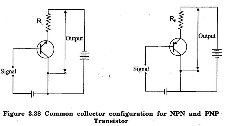
3. Common Collector configuration
Applications:
Current Gain or Current Amplification factor in CC Configuration
Relation between current gain γ and α:

Basic Electrical and Electronics Engineering: Unit III: Analog Electronics : Tag: : Three types, Operation, Characteristics, Circuit diagram | Bipolar Junction Transistors (BJT) - Transistor Configurations
Related Topics
Related Subjects

Basic Electrical and Electronics Engineering
BE3251 2nd semester Mechanical Dept | 2021 Regulation | 2nd Semester Mechanical Dept 2021 Regulation

Basic Electrical and Electronics Engineering
BE3251 2nd Semester CSE Dept 2021 | Regulation | 2nd Semester CSE Dept 2021 Regulation