Materials Science: Unit III: Semiconductors and Transport Physics
Schottky Diode
Definition, Symbol, Working Principle, Energy band diagram, VI Characteristics, Advantages, Applications
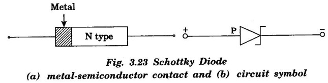
It is a junction formed between a metal and n-type semiconductor.
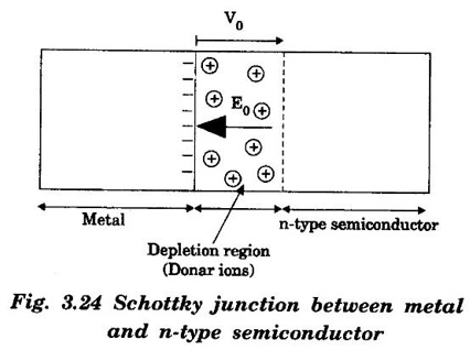
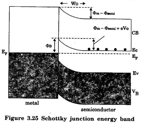
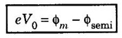
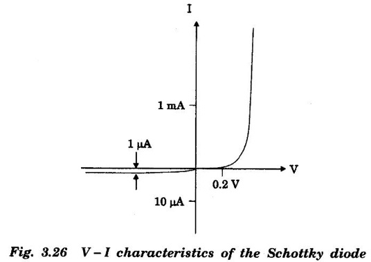
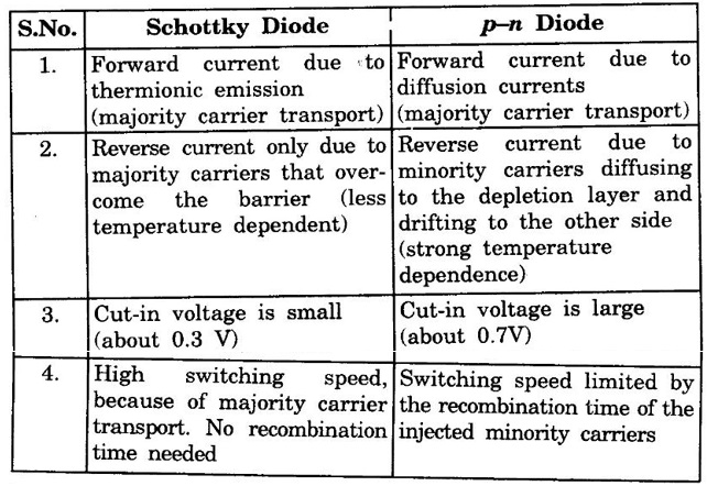
SCHOTTKY DIODE It is a junction formed between a metal and n-type semiconductor. When the metal has a higher work function than that of n-type semiconductor then the junction formed is called schottky diode. The Fermi level of the semiconductor is higher (since its work function is lower) than the metal. Fig. 3.23 shows schottky diode and its circuit symbol. The electrons in the conduction level of the semiconductor move to the empty energy states above the Fermi level of the metal. This leaves a positive charge on the semiconductor side and a negative charge (due to the excess electrons) on the metal side as shown in figure 3.24. This leads to a contact potential. When a Schottky junction is formed between metal and semiconductor, Fermi level lines up. Also a positive potential is formed on the semiconductor side. The formation of a depletion region of width WD within the semiconductor is shown in figure 3.25. Because the depletion region extends within a certain depth in the semiconductor, there is bending of the energy bands on the semiconductor side. Bands bend up in the direction of the electric field produced in depletion region. There is a built in potential V0 in the Schottky junction. From the figure 3.25, this is given by the difference in work functions. The contact potential thus formed prevents further motion of the electrons between the metal and semiconductor. This is called the Schottky barrier and denoted by ϕB. The behaviour of the schottky diode is further studied by biasing (applying voltage). The voltage is applied in two ways (a) Forward bias (b) Reverse bias In this bias, metal is connected to positive terminal and n-type semiconductor is connected to negative terminal of the battery. In the forward biased Schottky junction, the external potential opposes the in-built potential. The electrons injected from the external circuit into the n-type semiconductor have a lower barrier to overcome before reaching the metal. This leads to a current in the circuit which increases with increasing external potential. In reverse bias, metal is connected to negative terminal and n-type semiconductor to positive terminal of the battery. In the case of a reverse bias, the external potential is applied in the same direction as the junction potential. This increases the width of depletion region further and hence there is no flow of electron from semiconductor to metal. So a Schottky junction acts as a rectifier ie. it conducts in forward bias but not in reverse bias. The V-I characteristics of the junction is shown in figure 3.26. There is an exponential increase in current in the forward bias while there is a very small current in reverse bias. • In schottky diode, stored charges or depletion region is negligible. So a schottky diode has a very low capacitance. • In schottky diode, the depleting region is negligible. So the schottky diode will immediately switch from ON to OFF state (fast recovery time). • The depletion region is negligible in schottky diode. So applying a small voltage is enough to produce large current. • It has high efficiency. • It operates at high frequencies. • It produces less noise. • Schottky diode can be used for rectification of signals of frequencies even exceeding 300 MHz. • It is commonly used in switching device at frequencies of 20 GHz. • It is used in radio frequency (RF) applications. • It is widely used in power supplies. • It is used to detect signals. • It is used in logic circuits. • Its low noise figure finds application in sensitive communication receivers like radars. • It is also used in clipping and clamping circuits and in computer gating. Note: This diode is also referred as hot carrier diode because when it is forward biased, conduction electrons on the N side gains sufficient energy to cross the junction and enter the metal. Since these electrons enter into the metal with large energy, they are commonly called as hot carrier. Table 3.7Definition:
Energy band diagram
Working
(a) Forward bias
(b) Reverse bias
V-I Characteristics
Advantages of Schottky diode
Applications of Schottky diode
Differences between Schottky diode and p-n diode
Materials Science: Unit III: Semiconductors and Transport Physics : Tag: : Definition, Symbol, Working Principle, Energy band diagram, VI Characteristics, Advantages, Applications - Schottky Diode
Materials Science: Unit III: Semiconductors and Transport Physics
Under Subject
Materials Science
PH3251 2nd semester Mechanical Dept | 2021 Regulation | 2nd Semester Mechanical Dept 2021 Regulation
Related Subjects

Professional English II
HS3251 2nd Semester 2021 Regulation | 2nd Semester Common to all Dept 2021 Regulation

Statistics and Numerical Methods
MA3251 2nd Semester 2021 Regulation M2 Engineering Mathematics 2 | 2nd Semester Common to all Dept 2021 Regulation
Engineering Graphics
GE3251 eg 2nd semester | 2021 Regulation | 2nd Semester Common to all Dept 2021 Regulation
Physics for Electrical Engineering
PH3202 2nd Semester 2021 Regulation | 2nd Semester EEE Dept 2021 Regulation
Basic Civil and Mechanical Engineering
BE3255 2nd Semester 2021 Regulation | 2nd Semester EEE Dept 2021 Regulation
Electric Circuit Analysis
EE3251 2nd Semester 2021 Regulation | 2nd Semester EEE Dept 2021 Regulation

Physics for Electronics Engineering
PH3254 - Physics II - 2nd Semester - ECE Department - 2021 Regulation | 2nd Semester ECE Dept 2021 Regulation
Electrical and Instrumentation Engineering
BE3254 - 2nd Semester - ECE Dept - 2021 Regulation | 2nd Semester ECE Dept 2021 Regulation
Circuit Analysis
EC3251 - 2nd Semester - ECE Dept - 2021 Regulation | 2nd Semester ECE Dept 2021 Regulation
Materials Science
PH3251 2nd semester Mechanical Dept | 2021 Regulation | 2nd Semester Mechanical Dept 2021 Regulation

Basic Electrical and Electronics Engineering
BE3251 2nd semester Mechanical Dept | 2021 Regulation | 2nd Semester Mechanical Dept 2021 Regulation

Physics for Civil Engineering
PH3201 2021 Regulation | 2nd Semester Civil Dept 2021 Regulation
Basic Electrical, Electronics and Instrumentation Engineering
BE3252 2021 Regulation | 2nd Semester Civil Dept 2021 Regulation

Physics for Information Science
PH3256 2nd Semester CSE Dept | 2021 Regulation | 2nd Semester CSE Dept 2021 Regulation

Basic Electrical and Electronics Engineering
BE3251 2nd Semester CSE Dept 2021 | Regulation | 2nd Semester CSE Dept 2021 Regulation

Programming in C
CS3251 2nd Semester CSE Dept 2021 | Regulation | 2nd Semester CSE Dept 2021 Regulation