Materials Science: Unit III: Semiconductors and Transport Physics
Carrier Concentration in Intrinsic Semiconductors
Definition, Density of Electrons, Limitations
The number of electrons in conduction band per unit volume of the material is called as electron concentration (n).
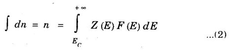
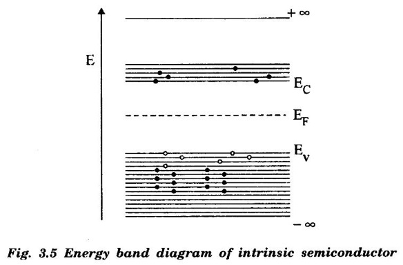
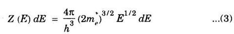
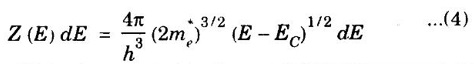
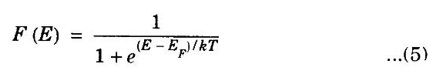
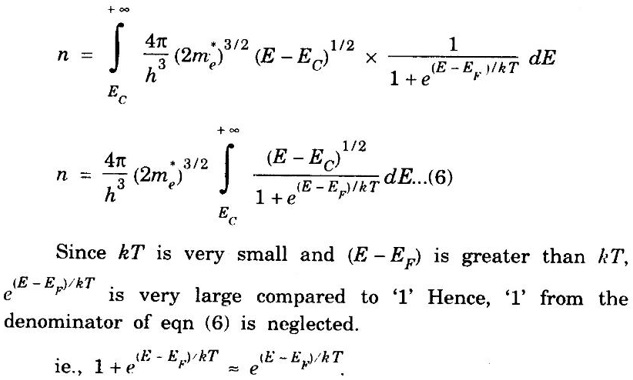
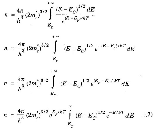
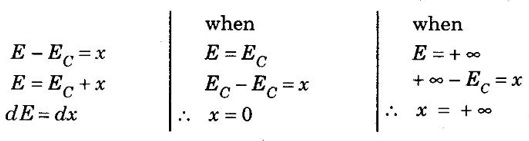
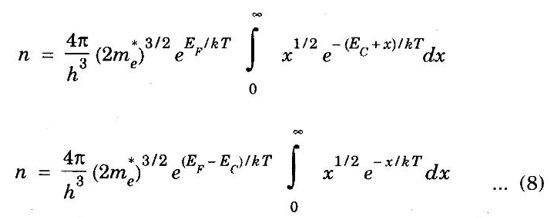
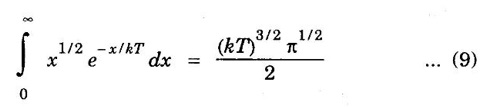
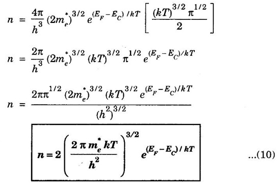
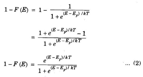
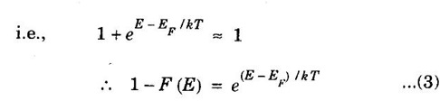
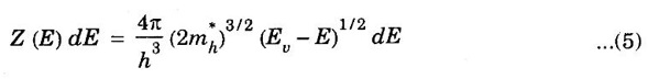
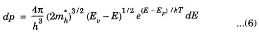
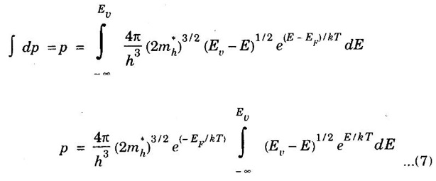
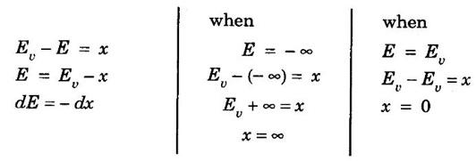
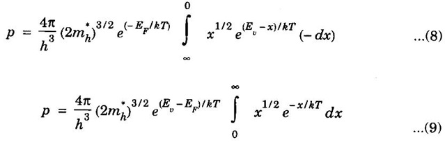
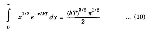
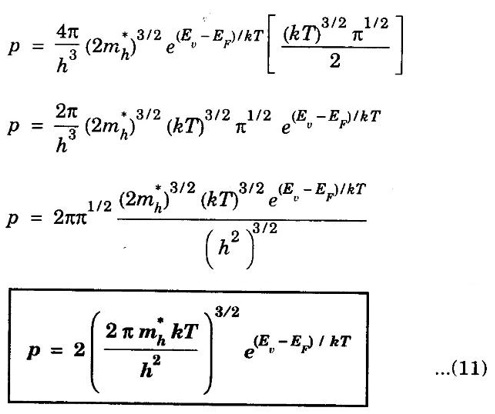
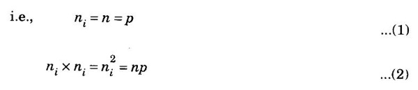
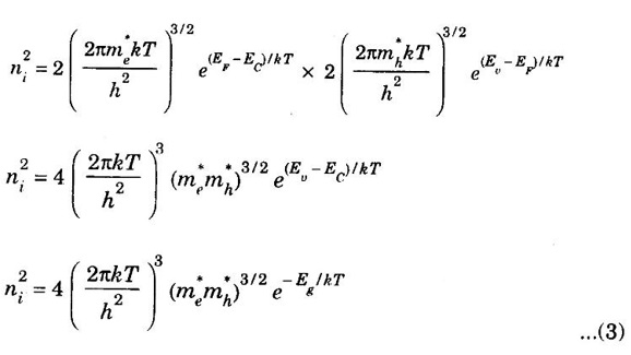
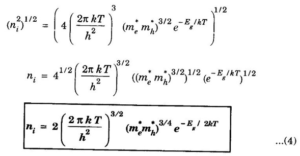
CARRIER CONCENTRATION IN INTRINSIC SEMICONDUCTORS The number of electrons in conduction band per unit volume of the material is called as electron concentration (n). Similarly the number of holes in valence band per unit volume of the material is called hole concentration (p). In general, the number of charge carriers per unit volume of the material is called carrier concentration. It is also known as density of charge carriers. The number of electrons per unit volume in conduction band for energy between E and E + dE is given by dn = Z (E) F (E) dE ...(1) where Z (E) dE - Density of states in energy between E and E + dE F (E) - Probability of electron occupancy. Number of electrons in conduction band for the entire range is calculated by integrating eqn (1) between energy Ec and + ∞. Ec is energy corresponding to the bottom most level and +∞ is energy corresponding to the upper most level in conduction band. (Fig 3.5). Density of states in conduction band between the energy range E and E + dE is given by The bottom edge of the conduction band (EC) denotes the potential energy of an electron at rest. Therefore, (E – EC) is the kinetic energy of conduction electron at higher energy levels. Thus, in eqn (3), E is replaced as (E – EC) The electrons in conduction band are not totally free. They move in a periodic potential of the crystal lattice. Therefore, in eqn (3), the mass of the electron (m) is replaced by its effective mass me* according to band theory of solids. The probability of electron occupation is given by Fermi distribution function Substituting eqns (4) and (5) in (2), we get Now, eqn (6) becomes To evaluate above integral in eqn (7), let us assume Substituting above values in eqn (7), we have Using the gamma function, it is shown that Substituting eqn (9) in eqn (8), we have Equation (10) is the expression for concentration of electrons in the conduction band of intrinsic semiconductor. Density of holes in Valence Band of Intrinsic Semiconductor (Derivation) We know that if an electron is transferred from valence band to conduction band, a hole is created in valence band. Let dp be the number of holes per unit volume in valence band between the energy E and E + dE. dp = Z (E) (1 - F (E)) dE ...(1) where Z (E) dE→ Density of states in the energy range E and E + dE. Since F(E) is the probability of electron occupation 1 - F (E) is the probability of an unoccupied electron state, i.e., probability of presence of hole. Since E is very small when compared to EF, in valenceband, (E - EF) is a negative quantity. Therefore, e (E – EF)/kT is very small and it is neglected in the denominator term of eqn (2). Density of states in valence band, Here, mh* is the effective mass of the hole in valence band. Ev, top of energy level in valence band is the potential energy of a hole at rest. Hence, (Ev - E) is the kinetic energy of the hole at level below Ev. So the term E in eqn (4) is replaced as (Ev - E). Substituting eqns (3) and (5) in (1), we get The number of holes in valence band for the entire energy range is obtained by integrating eqn (6) between limits - ∞ to Ev. To evaluate the integral in eqn (7), let us assume, Substituting these values in eqn (7), we have [-ve sign is omitted by interchanging the limits] Using the gamma function, it is shown that Substituting eqn (10) in eqn (9), we have The equation (11) is the expression for the concentration of holes in valence band of intrinsic semiconductor. In an intrinsic semiconductor, the number of electrons in conduction band is equal to the number of holes in valence band. In general, intrinsic carrier concentration ni is equal to electrons concentration concentration in conduction band (n) or holes concentration in valence band (p). Substituting the expressions of n and p in eqn (2), we have where EC - Ev = Eg is forbidden energy gap. Taking square root on both sides in eqn (3), we have The eqn (4) is expression for intrinsic carrier concentration Intrinsic semiconductors cannot be directly used to fabricate devices due to the following limitations: • Electrical conductivity is low. Germanium has a conductivity of 1.67Ω-1m-1 which is nearly 107 times smaller than that of copper. • Electrical conductivity is a function of temperature and increases exponentially as temperature increases. In intrinsic or pure semiconductors, the carrier concentration of both electrons and holes is very low at normal temperatures. In order to get sufficient current density density through semiconductor, a large electrical field should be applied. This problem is overcome by adding suitable impurities into intrinsic semiconductors.Definition
Density of Electrons in Conduction Band (Derivation)

INTRINSIC CARRIER CONCENTRATION
Limitations of intrinsic semiconductor
Materials Science: Unit III: Semiconductors and Transport Physics : Tag: : Definition, Density of Electrons, Limitations - Carrier Concentration in Intrinsic Semiconductors
Materials Science: Unit III: Semiconductors and Transport Physics
Under Subject
Materials Science
PH3251 2nd semester Mechanical Dept | 2021 Regulation | 2nd Semester Mechanical Dept 2021 Regulation
Related Subjects

Professional English II
HS3251 2nd Semester 2021 Regulation | 2nd Semester Common to all Dept 2021 Regulation
Statistics and Numerical Methods
MA3251 2nd Semester 2021 Regulation M2 Engineering Mathematics 2 | 2nd Semester Common to all Dept 2021 Regulation

Engineering Graphics
GE3251 eg 2nd semester | 2021 Regulation | 2nd Semester Common to all Dept 2021 Regulation
Physics for Electrical Engineering
PH3202 2nd Semester 2021 Regulation | 2nd Semester EEE Dept 2021 Regulation

Basic Civil and Mechanical Engineering
BE3255 2nd Semester 2021 Regulation | 2nd Semester EEE Dept 2021 Regulation
Electric Circuit Analysis
EE3251 2nd Semester 2021 Regulation | 2nd Semester EEE Dept 2021 Regulation

Physics for Electronics Engineering
PH3254 - Physics II - 2nd Semester - ECE Department - 2021 Regulation | 2nd Semester ECE Dept 2021 Regulation
Electrical and Instrumentation Engineering
BE3254 - 2nd Semester - ECE Dept - 2021 Regulation | 2nd Semester ECE Dept 2021 Regulation
Circuit Analysis
EC3251 - 2nd Semester - ECE Dept - 2021 Regulation | 2nd Semester ECE Dept 2021 Regulation
Materials Science
PH3251 2nd semester Mechanical Dept | 2021 Regulation | 2nd Semester Mechanical Dept 2021 Regulation

Basic Electrical and Electronics Engineering
BE3251 2nd semester Mechanical Dept | 2021 Regulation | 2nd Semester Mechanical Dept 2021 Regulation

Physics for Civil Engineering
PH3201 2021 Regulation | 2nd Semester Civil Dept 2021 Regulation
Basic Electrical, Electronics and Instrumentation Engineering
BE3252 2021 Regulation | 2nd Semester Civil Dept 2021 Regulation

Physics for Information Science
PH3256 2nd Semester CSE Dept | 2021 Regulation | 2nd Semester CSE Dept 2021 Regulation

Basic Electrical and Electronics Engineering
BE3251 2nd Semester CSE Dept 2021 | Regulation | 2nd Semester CSE Dept 2021 Regulation

Programming in C
CS3251 2nd Semester CSE Dept 2021 | Regulation | 2nd Semester CSE Dept 2021 Regulation