Basic Electrical and Electronics Engineering: Unit III: Analog Electronics
PN Junction
Symbol, Biasing, VI Characteristics, Important terms, Applications
P-type Semiconductor and N-type Semiconductor are chemically combined with a special fabrication technique to form a PN Junction.
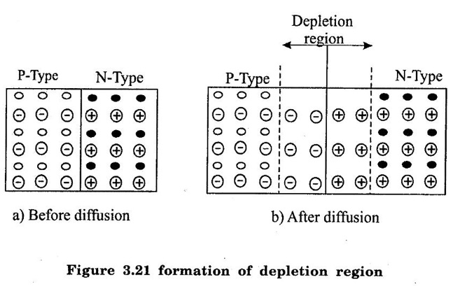
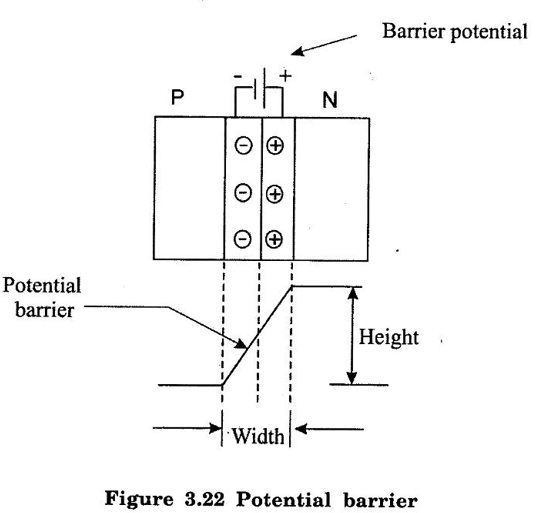
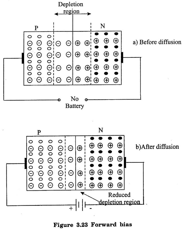
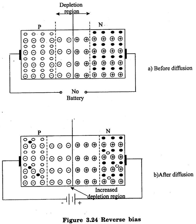
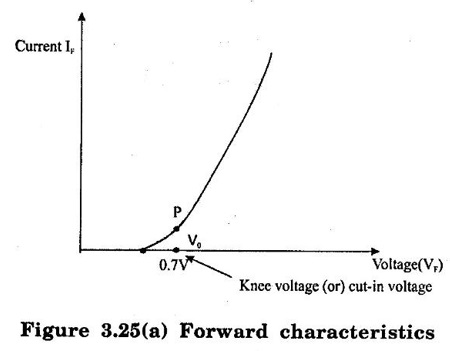
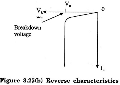
PN JUNCTION P-type Semiconductor and N-type Semiconductor are chemically combined with a special fabrication technique to form a PN Junction. When a germanium or silicon crystal contains donor impurities on one side and acceptor impurities on another side, a P-N junction is formed. The PN junction is very important device, because, all other semiconductor devices contains at least one PN junction. Figure 3.21 shows PN junction with formation of depletion region at the junction. The P-region contains a holes as majority carriers, electrons as minority carriers and negatively charged immobile ions (acceptor ions). The N- region contains electrons as majority carriers, holes as minority carriers and positively charged immobile ions (donor ions). The sample as a whole is electrically neutral and hence, P-region and N-regions considered separately. When the PN junction is formed, the following actions takes place. Some of the electrons from N-region (high carrier concentration) diffuse into the P- region (low carrier concentration). In P- region, they recombine with free holes. Similarly some of the holes from P- region (high carrier concentration) diffuse into the N-region (low carrier concentration). In N-region, they recombine with free electrons. The P-region contains more number of holes and N-region contains more number of electrons, so there is a concentration difference in two regions. Since this concentration difference, a large concentration gradient is exists across the junction. Besides this, electrons and holes move at random in all directions because of thermal energy. This diffusion process across the junction takes place only for a short time. After a few recombination of electrons and holes, the electrons in the N-region are neutralized by holes. Therefore, the positive immobile ions (donor) are left behind in this small region. Similarly holes in the P-region are neutralised by electrons. Therefore, the negative immobile ion (acceptor) are left behind in this small region. These immobile ions are fixed in their positions and they are electrically charged. Those immobile ions forms the parallel rows or plates of opposite charges facing each other across the depletion layer. The depletion region is also called as space charge region. "When PN junction is formed, there exist a region at the junction which is depleted of mobile charges called as "depletion region (or) transition region" (or) space charge region." An electric field exists across the junction due to immobile positive and negative ions on opposite sides of the junction. This electric field is called as "barrier potential". The polarities of barrier potential is depends on types of the immobile ions present on two sides of the junction. i.e, the positive terminal of barrier potential on N side and the negative terminal of the barrier potential on P side as shown in figure 3.22. Barrier potential act as a barrier which oppose the flow of electrons and holes to cross the junction till the external voltage applied. Barrier potential is 0.7 volt for silicon and 0.3 volt for germanium. "When we apply external de supply across the PN junction, this process is called biasing of PN junction. The applied external de voltage controls the width of the depletion region." The PN junction can be biased in two ways. 1. Forward bias 2. Reverse bias 1. Forward bias. If the positive terminal of the battery is connected to P-side and negative terminal of the battery is connected to N-side, the junction is said to be forward biased (refer figure 3.23). Under forward biased condition, hole are repelled from the positive terminal of the battery and they are moves towards the junction. Likewise, electrons are repelled from negative terminal of the battery and they are move towards the junction. Some holes and electrons enter into the depletion region, it is because, holes and electrons have acquired energy from voltage source. This reduces the width of the depletion region. If applied voltage gradually increased from zero, the barrier potential also gets reduced gradually. As a result of this diffusion of more majority carriers across the junction. It causes a large current flows through the junction. This current is called as "forward current". If the positive terminal of the battery is connected to N-side and negative terminal of the battery is connected to P-side, then the junction is said to be reverse biased. (refer figure 3.24) Under reverse bias condition, the holes in the P-region are attracted by the negative terminal of the battery and the electrons in the N-region are attracted by the positive terminal of the battery. Hence majority carriers are flow away from the junction and results in width of depletion layer will be wider. This increases the barrier potential. Due to wider barriers potential, majority charge carriers are not able to cross over the junction. So no current flows due to majority charge carriers. But there are few thermally generated minority carriers present in both regions. The increased barrier potential, enhances small of amount of current flow due to minority carriers. This current is called as "reverse saturation current". If reverse bias voltage increased further, the kinetic energy of minority carriers become large enough to knock out electrons from atoms. At this point "breakdown" of the junction occurs, with sudden rise in reverse current. "A PN junction is a unilateral device. It offers a low resistance when forward biased and act as insulator when reverse biased." Forward Characteristics: A typical VI characteristics of forward biased PN junction diode is shown in figure 3.25(a). The forward current is increases with applied forward de voltage. The forward current is very small till the applied voltages reach the barrier potential (V0). Once the applied voltage is slightly greater than barrier potential, the forward current increases (IF) sharply. This point 'P' is known as knee voltage (or) cut in voltage. If the forward voltage(VF) increased beyond a certain specified value, the diode will burn due to overheat. A typical VI Characteristics of reverse biased pn junction diode is shown in figure 3.25(b). If the reverse voltage (VR) is increased from zero, very small amount of diode current will flow till it reaches breakdown voltage. This current is called as reverse saturation current I0(μA). If a large reverse bias voltage is applied, junction breakdown occurs. Due to this, diode reverse current increases rapidly. "The applied reverse bias voltage at which break down occurs is called as breakdown voltage (VB)." 1. Breakdown voltage: Under reverse biased condition, very small amount of reverse current (or) diode current will flow through a PN junction. If increasing the reverse bias voltage, a point may reach at which the junction breaks down with sudden rise in reverse current. The applied reverse bias voltage at which breakdown occur with sudden rise in reverse current is called as breakdown voltage. 2. Knee voltage: Under forward bias condition, forward current is very small till the applied voltage reach the barrier potential. The forward voltage, at which the forward current through the junction starts increasing rapidly is called as knee voltage (or) cut in voltage. 3. Peak inverse voltage: It is the maximum reverse voltage that can be applied to the PN junction without damage to the junction. If the reverse voltage exceeds its peak inverse voltage (PIV), the junction may get destroyed due to overheat. 4. Maximum power rating: The maximum value of power, which a diode can dissipate without any damage to it, is called maximum power rating. ● Used as rectifiers ● Used as switches ● Used in power supply circuits ● Used in clipper and clamper circuits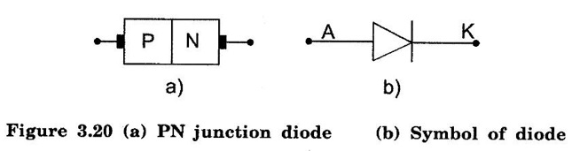
1. Depletion region formation:
2. Barrier Potential:
3. Biasing the PN junction
2. Reverse bias:
4. VI Characteristics of PN junction diode
Reverse Characteristics:
5. Important terms
6. Applications of PN junction diode
Basic Electrical and Electronics Engineering: Unit III: Analog Electronics : Tag: : Symbol, Biasing, VI Characteristics, Important terms, Applications - PN Junction
Related Topics
Related Subjects

Basic Electrical and Electronics Engineering
BE3251 2nd semester Mechanical Dept | 2021 Regulation | 2nd Semester Mechanical Dept 2021 Regulation

Basic Electrical and Electronics Engineering
BE3251 2nd Semester CSE Dept 2021 | Regulation | 2nd Semester CSE Dept 2021 Regulation