Basic Electrical and Electronics Engineering: Unit III: Analog Electronics
Metal Oxide Semiconductor Fet
Construction, Operation Working Principle, Classification, Symbol, Biasing, VI Characteristics, Applications
MOSFET is a three terminal semiconductor device.
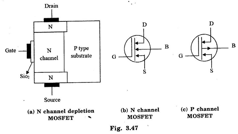
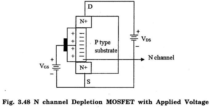
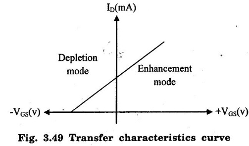
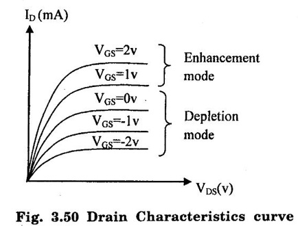
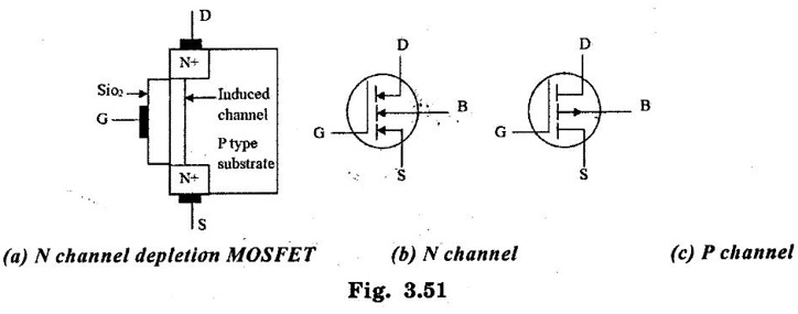
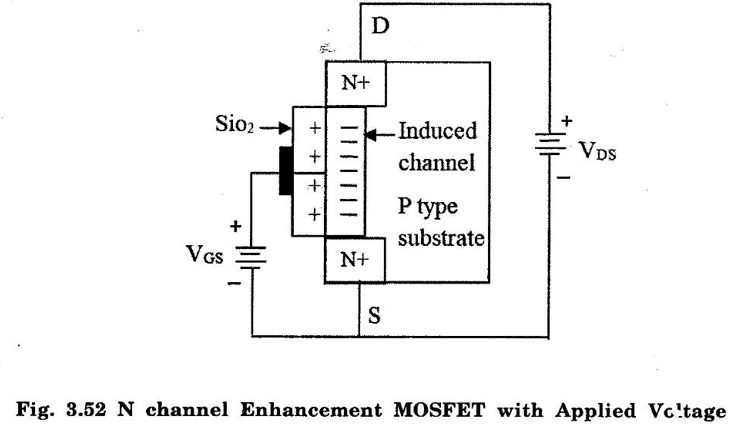
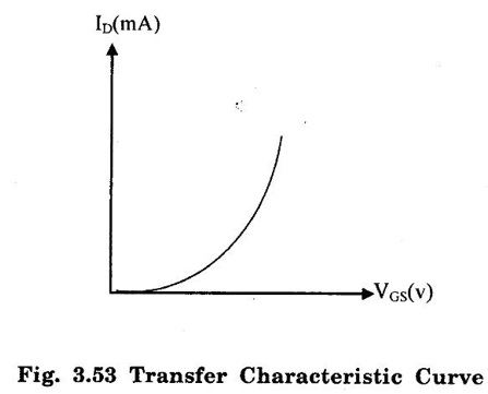
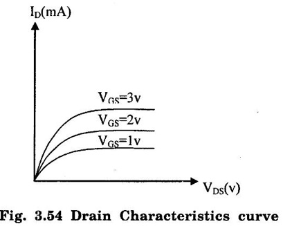
METAL OXIDE SEMICONDUCTOR FET: MOSFET is a three terminal semiconductor device. It is also known as Insulated Gate FET (IGFET) in which there is no pn junction structure, but instead the gate is insulated from the channel by oxide layer of SiO2 hence the name Insulated Gate FET. The electric field applied cross an insulated gate controls the majority carrier in the channel. There are two types of MOSFET (a) Depletion MOSFET (i) N channel D- MOSFET (ii) P channel D -MOSFET (b) Enhancement MOSFET (i) N channel E- MOSFET (ii) P channel E -MOSFET Construction:- In this N channel MOSFET, two heavily doped regions (Drain and source) of n type is diffused on the p type substrate. This diffused N type region is joined by the channel of n type. A thin layer of SiO2 layer is grown over the surface of the substrate and a thin layer of metal aluminum is placed over the SiO2 layer. This makes the gate which is connected to metal is insulated from channel hence the name IGFET. Operation:- The operation of the depletion mosfet is based on two modes. ● If Vps is applied, the electron from the source will moves towards the drain through the channel constitutes the current ID. ● If VGS is made negative, the induced negative charge will accumulate on the Sio2, attract the positive charge on the channel. This hole will deplete the mobile electron in channel. ● hence increasing VGS will reduce Current ID. If VGS is made positive, the induced positive charge will accumulate on the SiO2 attract the negative charge on the channel. This electron helps to increase the current ID. Characteristics:- MOSFET exhibit two characteristics: The graph drawn between ID and VGS is known as transfer characteristics. The value of IDSS will be Ipss though the Gate voltage Vgs is not applied, the increase in Vds will constitute Current ID. If VGS is positive, the value of ID will increase from IDSS. If VGS is negative, the value of ID will decrease from IDSS and will reach zero. ● The graph drawn between ID and VDS is known as drain characteristics. ● The value of ID increases with VDS, keeping increases in VGS (positively). This is known as enhancement mode. ● The value of ID decreases with VDS, keeping decreases in VGS (negatively) this is known as Depletion mode. In the n channel Enhancement MOSFET, two heavily doped N- type layers (Source and Drain) is diffused on the p type substrate but there is no channel between the n type layer as in the case of depletion MOSFET. One n+ region is connected to Drain and other to the source. A thin layer of SiO2 is deposited on the surface of the structure. An aluminium metal is placed over the SiO2 layer which forms the gate. Operation:- ● The operation of the enhancement MOSFET is based on enhancement mode only ● When VGS is applied positively, the negative charge will be accumulated near the SiO2 layer. ● This negative charge due to the attraction of +ve charge in the Sio2 layer will accumulate and form a layer known as induced inversion layer of negative carrier. ● When VDS is applied, the conductivity increases constitute current ID. Characteristics: Enhancement MOSFET exhibit two characteristics. Transfer characteristic: The graph drawn between ID and VGS is known a transfer characteristic. The characteristics curve is obtained in the positive region only. When VGS is increased ID increases with VGS. Drain characteristics:- The graph drawn between ID and VDS is known as drain characteristics with increases in the value of VDS, ID increases keeping increases in the value if VGS. (1) MOSFET is commonly preferred for implementing Logic gate. Hence it is widely used in switch, microprocessor, memory element etc. (ii) It is used as a discrete device in switch mode power supplies (SMPS), driven circuit etc. (iii) In the frequency driven circuit, it is used as a mixer and oscillator. (iv) It is used as a chopper amplifier and stabilization circuit in op-amp. (v) It functions as a switched capacitor circuits in time processing system.Categories of MOSFET:-
1. Depletion MOSFET
Depletion mode:-
Enhancement mode:-
Transfer characteristics:
Drain characteristics:-
2. Enhancement MOSFET:-
Application of MOSFET:
Basic Electrical and Electronics Engineering: Unit III: Analog Electronics : Tag: : Construction, Operation Working Principle, Classification, Symbol, Biasing, VI Characteristics, Applications - Metal Oxide Semiconductor Fet
Related Topics
Related Subjects

Basic Electrical and Electronics Engineering
BE3251 2nd semester Mechanical Dept | 2021 Regulation | 2nd Semester Mechanical Dept 2021 Regulation

Basic Electrical and Electronics Engineering
BE3251 2nd Semester CSE Dept 2021 | Regulation | 2nd Semester CSE Dept 2021 Regulation