Basic Electrical and Electronics Engineering: Unit III: Analog Electronics
JFET
Construction, Operation Working Principle, Classification, Symbol, Biasing, VI Characteristics, Applications
The junction field-effect transistor is the simplest type of field-effect transistor.
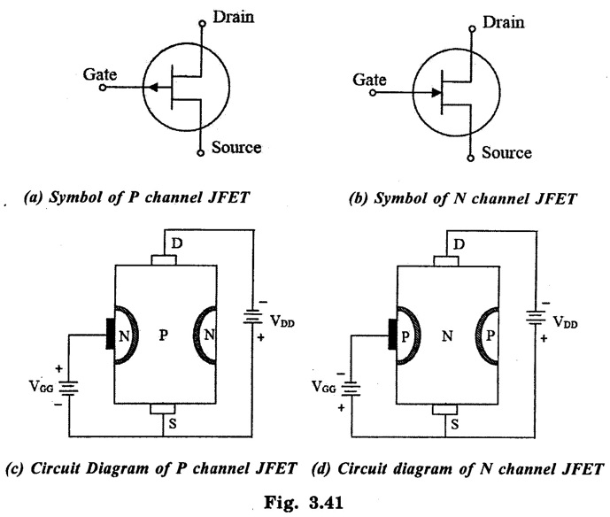
JFET The junction field-effect transistor is the simplest type of field-effect transistor. It is a three-terminal semiconductor device which can be used as a voltage-controlled resistance or as an electronically-controlled switch by controlling the flow of current by input voltage. Based on the majority carrier, JFET is further classified into (i) N channel JFET – electron is the majority carriers (ii) P channel JFET - holes is the majority carriers ● JFET consists of a p-type (or) N-type silicon channel. If the channel of the JFET is formed by P type silicon
channel then it is known as p type JFET. If the channel of the JFET is formed by N type silicon
channel then it is known as N type JFET. ● It has three terminals - Source, Drain and Gate. Source:- It is the terminal through which the majority carrier
enters the channel. Drain:- It is the terminal through which the majority carrier
leaves the channel. Gate:-
This is a heavily doped, internally connected two
sided region which is formed by diffusion process on both side of either p-type
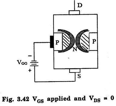
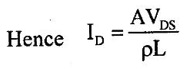
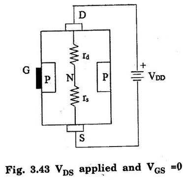
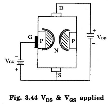
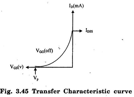
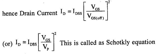
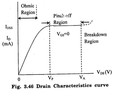
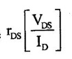
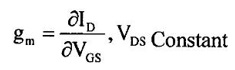
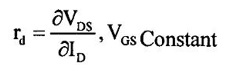
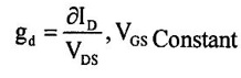
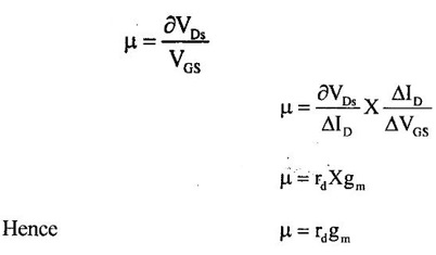
(or) n-type channel. Channel:- It is the N type (or) P- type semiconductor region between the two gates regions through which the majority carrier moves from source to drain constitute drain current. P Channel JFET:- In the P channel JFET, a p type bar of semiconductor material is taken. On the opposite faces of middle region, heavily doped n type region is diffused. Ohmic contacts are placed on the both end of the opposite faces to gates. One ohime contact is called source and other is drain N-Channel JFET:- In the N-Channel JFET, a n type bar of semiconductor material is taken. On the opposite faces of middle region, heavily doped p-type region is diffused. Ohmic contacts are placed on both opposite end faces to gates. One ohmie contact is called source and other is drain. Consider the N-Channel JFET in which VGG is applied between Gate and Source which is reverse biased and VDD is applied between source and drain where positive is applied at drain and negative is applied at source. The operation of JFET depends on three conditions. (i) VGS applied and VDS = 0 When the reverse bias is applied between Gate and Source the depletion region is formed due to the diffusion of electron in p type and holes in n-type region. If no VDD is applied this depletion region extends symmetrically, due to this Conductivity ID is zero. (ii) VDS applied and VGS = 0 When VGS=0 and the voltage is applied between drain and source. The electron will flow from drain to source and constitute the current known as ID. The current magnitude depends upon the following factors. 1) Number of majority carriers (electron in N type) available in the channel (ñ) 2) Length of the channel (L) 3) Cross sectional area of channel (n) 4) Applied voltage magnitude (VDS) There will be a resistance offered by drain and source which is represented as rd and rs. The voltage drop across Vrd>>Vrs. (iii) VDS & VGS applied When voltage is applied between drain and source, electron flows from source to drain constitutes Drain current ID. When the voltage which is applied between Gate and Source increases, the depletion region formed will reduces the current ID. When the VGG is further increases, the two depletion regions touch each other. It is called pinch off region. Thus by increasing VGG the current ID reduces to zero. Hence by means of voltage VGG, we can control the flow of electron (Current) ID in the output therefore JFET is known as voltage controlled device. JFET shows two important characteristics. (i) Transfer characteristic This characteristic is used to relate the VGS and ID. The graph is drawn between VGS and ID by increasing the value of VGG keeping suitable VDD value. Initially the value of ID is maximum it is given as IDD. When the value of VGS is increased, the value of ID decrease and reaches zero at the voltage known as pinch off voltage VP (or) VGS(off) (ii) Drain Characteristic This characteristic shows the relationship between Drain current (ID) and Drain to source voltage (VDS). ● When VDS is increases, ID increases the rate of increases in ID till point A is in linear manner. This region of curve is known as ohmie region. The resistance ● At point A, ID is maximum it is given as IDSS. When VDS is further increased the value of ID remains unchanged and maintains saturated state due to increases in VP. ● After point B, the drain current ID increases rapidly. This is due to breakdown in gate to source junction due to avalanche effect. This region is known as breakdown region and voltage at this point is known as breakdown voltage. The four important factors of the JFET is (i) Transconductance (or) mutual conductance (gm):- It is the ratio of a small change in Drain current ID to the small change in gate to source voltage, keeping VDS constant. Its unit is mho (ii) Drain Resistance (rd):- It is the ratio of a small change in drain to source voltage to the small change in drain current, keeping VGS constant. Its unit is ohms. (iii) Drain Conductance (gd):- It is the ratio of a small change in Drain current to drain to source voltage, keeping VGS constant (iv) Amplification Factor (m):- It is the ratio of a small change in drain to source voltage to the small change in gate to source voltage, keeping ID constant (i) Since JFET is voltage controlled device, it is used as a voltage variable resistor in voltage control circuits, operation amplifiers etc. (ii) JFET can be used as an amplifier element in buffer amplifier, Rf amplifier tuner circuit, operational amplifier etc. (iii) Due to its Voltage Variable Resistor function. It is used in an Automatic Gain Control Circuits. It is used as a mixer and oscillator in various frequency driven circuits.Construction of JFET:-
2. Operation of JFET:-
3. Characteristics of JFET
 is related to gate to source voltage (VGS) in linear manner.
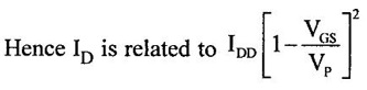
Characteristics parameters of JFET
Application of JFET:
Basic Electrical and Electronics Engineering: Unit III: Analog Electronics : Tag: : Construction, Operation Working Principle, Classification, Symbol, Biasing, VI Characteristics, Applications - JFET
Related Topics
Related Subjects

Basic Electrical and Electronics Engineering
BE3251 2nd semester Mechanical Dept | 2021 Regulation | 2nd Semester Mechanical Dept 2021 Regulation

Basic Electrical and Electronics Engineering
BE3251 2nd Semester CSE Dept 2021 | Regulation | 2nd Semester CSE Dept 2021 Regulation