Basic Electrical and Electronics Engineering: Unit III: Analog Electronics
Full Wave Rectifier
Construction, Operation Working Principle, Circuit Diagram, Waveform, Formula, Calculation
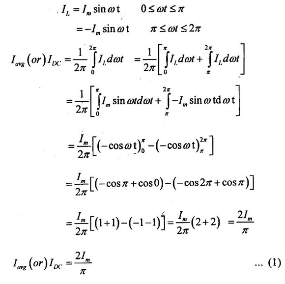
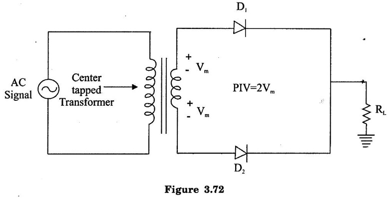
Figure (3.70) shows centre tapped full wave rectifier. In full wave rectifier, the rectifying element conducts in both positive and negative cycles of the input signal.
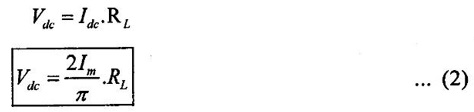
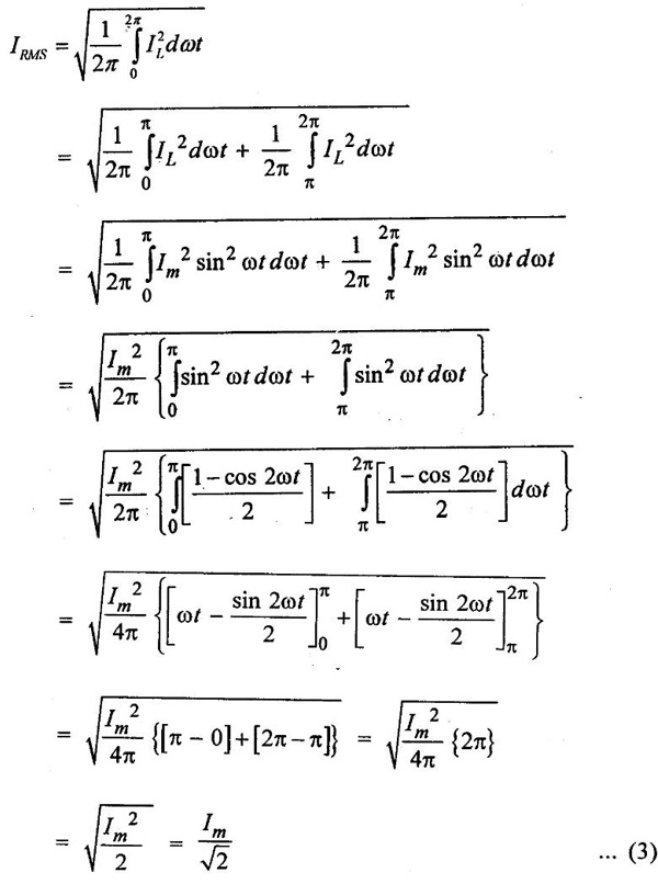
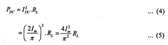
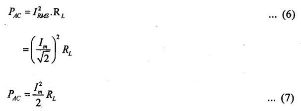
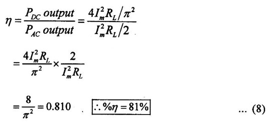
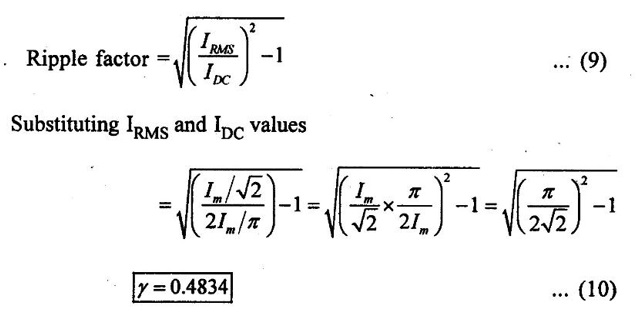
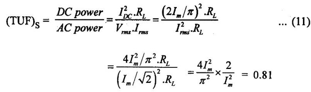
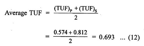
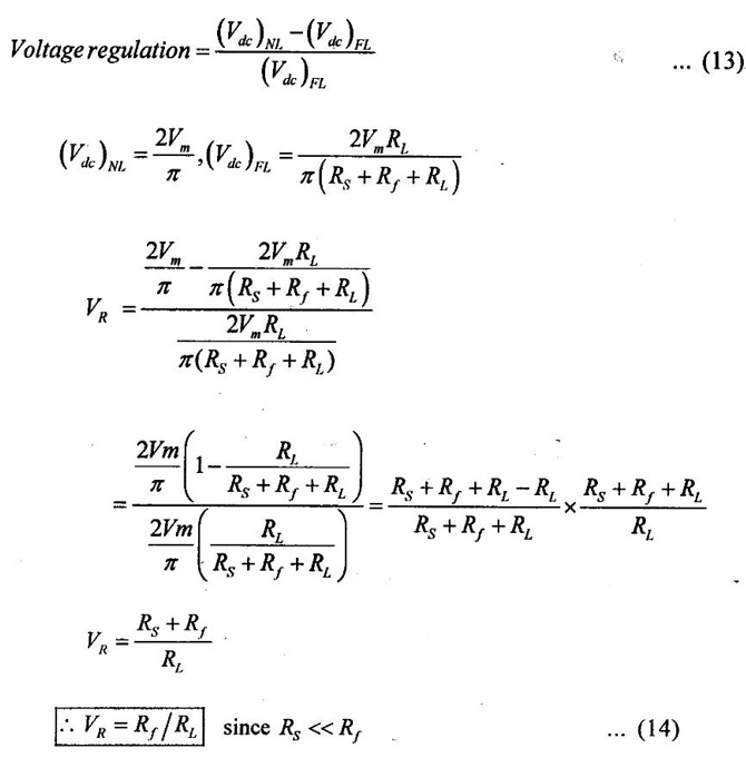
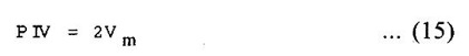
FULL WAVE RECTIFIER Figure (3.70) shows centre tapped full wave rectifier. In full wave rectifier, the rectifying element conducts in both positive and negative cycles of the input signal. Due to centre tapping, the impedance of the two halves of windings are equal. Hence, the voltages in two halves are 180° out of phase. During positive half cycle of input, the D1 is conducts and D2 is in off state. The current flows through the load resistor RL While negative half cycle of input, D2 conducts and D1 is in off state. The current flows through the load resistor RL. Consider one cycle of load current IL from 0 to 2л to obtain the average value which is dc value of load current. The dc voltage is, The RMS value of current can be obtained as follows, DC power output written as, AC power input written as, This is the maximum theoretical efficiency of full wave rectifier. (i.e.) efficiency of full wave rectifier is twice times of half wave rectifier efficiency. As derived earlier in case of half wave rectifier the ripple factor is given by a general expression, In full wave rectifier, the secondary current flows through each half separately in every half cycle, while the primary of transformer carries current continuously. Hence TUF is calculated for primary and secondary windings separately and then the average TUF is determined. For secondary, We know that a full wave rectifier consists of two half wave rectifiers. Therefore, TUF for primary = 2 × TUF of HWR (TUF)P = 2 × 0.287 = 0.574 For full wave circuit, Peak inverse voltage of full wave rectifier is twice the value of Half wave rectifier, Circuit diagram for peak inverse voltage: Disadvantage of Full wave Rectifier Design and maintenance of center tapped transformer is difficult.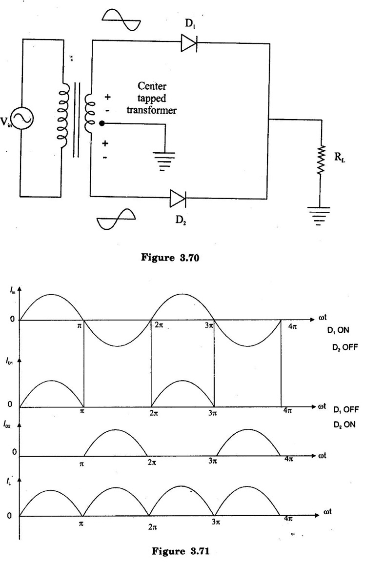
1. Average DC Load Current (IDC)
2. Average (or) DC load voltage (VDC)
3. RMS Load Current (IRMS)
4. DC Power Output (PDC)
5. AC Power input (PAC)
6. Rectifier Efficiency (η)
7. Ripple Factor
8. Transformer Utilization Factor (TUF)
9. Voltage Regulation
10. Peak inverse Voltage of Full Wave Rectifier.
Basic Electrical and Electronics Engineering: Unit III: Analog Electronics : Tag: : Construction, Operation Working Principle, Circuit Diagram, Waveform, Formula, Calculation - Full Wave Rectifier
Related Topics
Related Subjects

Basic Electrical and Electronics Engineering
BE3251 2nd semester Mechanical Dept | 2021 Regulation | 2nd Semester Mechanical Dept 2021 Regulation

Basic Electrical and Electronics Engineering
BE3251 2nd Semester CSE Dept 2021 | Regulation | 2nd Semester CSE Dept 2021 Regulation