Materials Science: Unit III: Semiconductors and Transport Physics
Additional 2 Marks Question & Answers
Semiconductors and Transport Physics | Materials Science
Additional 2 Marks Question & Answers: Semiconductors and Transport Physics - Materials Science
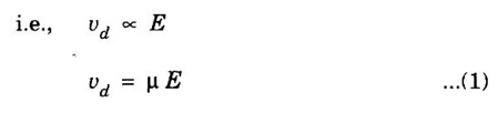
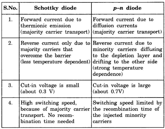
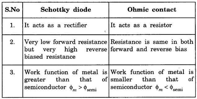
ADDITIONAL Q&A 1. What is a semiconductor? Semiconductor is a special class of material which behaves like an insulator at 0 K and acts as conductor at temperature other than 0 K. Its resistivity lies in between a conductor and an insulator. 2. Draw the energy level diagram of a semiconductor. 3. What is an intrinsic semiconductor? Semiconductor in an extremely pure form (without impurities) is known as intrinsic semiconductor. 4. What is an extrinsic semiconductor? A semiconducting material in which impurity atoms added (doped) to the material to modify its conductivity is known as extrinsic semiconductor or impurity semiconductor. 5. What is an n-type semiconductor? When a small amount of pentavalent impurity is added to pure semiconductor, it becomes extrinsic or semiconductor and it is known as n-type semiconductor. 6. What is a p-type semiconductor? When a small amount of trivalent impurity is added to a pure semiconductor, it becomes extrinsic semiconductor or impure semiconductor and it is called p-type semiconductor. 7. What is meant by doping and doping agent? The technique of adding impurities to a pure semiconductor is known as doping and the added impurity is called doping agent. 8. Explain the concept of hole in semiconductor. In intrinsic semiconductor, charge carriers are created due to breaking of covalent bonds. When a covalent bond is broken, an electron escapes to the conduction band leaving behind an empty space in the valence band. This missing electron is called a hole. 9. What is meant by donor energy level? A pentavalent impurity when doped with an intrinsic semiconductor donates one electron which produces an energy level called donor energy level. 10. What is meant by acceptor energy level? A trivalent impurity when doped with an intrinsic semiconductor accepts one electron which produces an energy level called acceptor energy level. 11. Mention the uses of compound semiconductor. They are used as photovoltaic materials, photoconductive cell, laser materials and for making LED (Light Emitting Diode]. 12. Define drift velocity. When an electrical field is applied in a semiconducting material, the free charge carriers such as free electrons and holes attain drift velocity vď The drift velocity attained by the carriers is proportional to the electrical field strength E. where μ is a proportionality constant and it is known as the mobility of the charge carrier. 13. Define drift current. The electric current produced due to the motion of charge carriers under the influence of an external electric field is known as drift current. 14. Define diffusion current. The non-uniform distribution of charge carriers creates the regions of uneven concentrations in the semiconductor. The charge carriers move from the regions of higher concentration to the regions of lower concentration. This process is known as diffusion. The current is known as diffusion current. 15. What is a Hall device? The device which uses the hall effect for its application is known as Hall device. 16. What are different types of Hall devices? There are three types of Hall devices. They are (a) Gauss Meter (b) Electronic Multiplier (c) Electronic Wattmeter 17. What is a schottky diode? It is a junction formed between a metal and n-type semiconductor. When the metal has a higher work function than that of n-type semiconductor then the junction formed is called schottky diode. 18. What are advantages of schottky diodes? • In schottky diode, stored charges or depletion region is negligible. So a schottky diode has a very low capacitance. • In schottky diode, the depleting region is negligible. So the schottky diode will immediately switch from ON to OFF state (fast recovery time). • The depletion region is negligible in schottky diode. So applying a small voltage is enough to produce large current. • It has high efficiency. • It operates at high frequencies. • It produces less noise. 19. What are the application of scholtky diode? • Schottky diode can be used for rectification of signals of frequencies even exceeding 300 MHz. • It is commonly used in switching device at frequencies of 20 GHz. • It is used in radio frequency (RF) applications. • It is widely used in power supplies. 20. What is ohmic contact? An ohmic contact is a type of metal semiconductor junction. It is formed by a contact of a metal with a heavily doped semiconductor. When the semiconductor has a higher work function than that of metal, then the junction formed is called the Ohmic junction. 21. What are the differences between schottky diode and p-n diode? 22. What are the differences between schottky diode and ohmic contacts? 23. What are the uses of ohmic contact? The use of ohmic contacts is to connect one semiconductor device to another, an IC, or to connect an IC to its external terminals.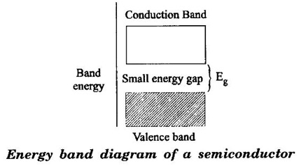
Materials Science: Unit III: Semiconductors and Transport Physics : Tag: : Semiconductors and Transport Physics | Materials Science - Additional 2 Marks Question & Answers
Related Topics
Related Subjects
Materials Science
PH3251 2nd semester Mechanical Dept | 2021 Regulation | 2nd Semester Mechanical Dept 2021 Regulation