Engineering Materials and Metallurgy: Unit 0: Review of Crystal Physics
Surface Defects (or plane defects)
Definition, Types, Examples | Crystal Physics
The defects, which takes place on the surface of a material are known as surface defects or plane defects.
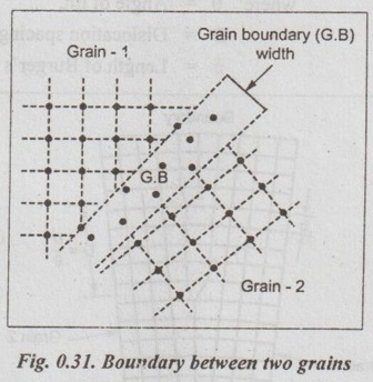
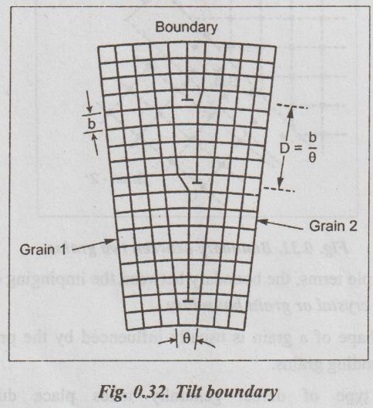
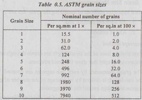
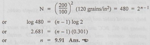
SURFACE DEFECTS (OR PLANE DEFECTS) ✓ The defects, which takes place on the surface of a material are known as surface defects or plane defects. ✓ They are also called as two dimensional surface imperfections. ✓ They are caused due to the change in the stacking of atomic planes across boundary. * The burgers vector is the vector, which defines the magnitude and the direction of slip. ✓ The different types of surface defects are: 1. Grain boundary, 2. Tilt or twist boundary, 3. Twin boundary, and 4. Stacking fault. ✓ Whenever grains of different orientation separate the general pattern of atoms and exhibits a boundary, as shown in Fig.0.31, the defect caused is known as grain boundary. ✓ In simple terms, the boundary between the impinging crystals is called crystal or grain boundary. ✓ The shape of a grain is usually influenced by the presence of surrounding grains. ✓ This type of defect generally takes place during the solidification of the liquid metal. ✓ Tilt boundaries are low angle (i.e., less than 10°) grain boundaries and are considered as an array of parallel edge dislocations of same sign (i.e., either T or ⊥) arranged one above the other in an array or series, as shown in Fig.0.32. ✓ The angle of tilt is given by, tan θ = b/D when θ is very small, then tan θ ≈ θ ⸫ θ = b/D where θ = Angle of tilt, D = Dislocation spacing, and b = Length of Burger's vector. ✓ Twist Boundaries are also low angle grain boundaries. It consists of atleast two sets of parallel screw dislocations lying in the boundary. The two important methods of measuring the grain size are : 1. An intercept method, and 2. ASTM method. 1. An intercept method ✓ First straight lines of the equal length are drawn through several photomicrographs that show the grain structure. ✓ The grains intersected by each line segment are counted. Then the line length is divided by an average of the number of grains intersected, taken overall the line segments. ✓ The average grain diameter is found by dividing this result by the linear magnification of the photomicrographs. 2. ASTM method ✓ The most widely accepted measure of the grain size is the American Society for Testing and Materials (ASTM) method. ✓ The ASTM defines the grain-size number (n) through the equation : where N = Number of grains per square inch on a polished and etched material surface at a magnification of 100 ×, and n = ASTM grain-size number ✓ Grain-size numbers with the nominal number of grains per square inch at 100 × and grains per square millimeter at 1 × are listed in Table 0.5. ✓ The grain size (n) is essentially an index of the fineness of the structure. Thus as the grain size (n) increases, the structure becomes increasingly fine. ✓ Typically a fine-grained material will have an ASTM grain size of 8 to 10 while coarse-grained materials have grain sizes on the order of 2 or 3. Example 0.1 An ASTM grain size determination is being made from a photomicrograph of a metal at a magnification of 100 × What is the ASTM grain-size number of the metal if there are 128 grains per square inch? ● Solution: We know that, N = 2n-1 where N = Number of grains per square inch at 100 ×, and n = ASTM grain-size number 128 grains/in2 = 2n-1 or log 128 = (n – 1) (log 2) or 2.107 = (n – 1) (0.301) or n = 8 Ans. Example 0.2 If there are 120 grains per square inch on a photomicrograph of a metal at 200 ×, what is the ASTM grain-size number of the metal? ● Solution: If there are 120 grains/in2 at 200 ×, then at 100 ×, we will have ✔ Solids are classified into three groups on the basis of atomic arrangement. They are single crystals, polycrystalline materials and amorphous substances. ✔ Atomic arrangement in crystalline solids is described by a space lattice. A space lattice is a three dimensional array of points each of which has identical environment. ✔ A unit cell is the most convenient small cell in a crystal structure that carries the characteristics of the crystal. The repetition of the unit cell in three dimensions generate the whole crystal structure. ✔ A unit cell is characterised by three axial lengths (a, b, c) and three axial angles (α, β, γ). ✔ Lattice parameters are: (a) The lengths of the sides (a, b, c) of the unit cell, and (b) The angles (α, β, γ) between the sides. ✔ The single crystals are classified into 7 crystal systems. The seven systems have a total of 14 unit cells based on the internal arrangement of atomic sites within the unit cell. ✔ Presence of a large vacancy or void such as clusters of atoms missing is also considered as a volume imperfection. ✔ Usually interferometric techniques are used to analyse the volume defects. ✔ Among the seven crystal systems, the cubic system is the simplest and possess symmetry of high order. ✔ The cubic system has three types of unit cells: Simple cubic, body centred cubic and face centred cubic. ✔ Among the SC, BCC and FCC cells, the FCC cell has more particle content and closely packed. About 29 metals crystallize in this structure. BCC structure is exhibited by about 20 metals. Only one element polonium exhibits SC structure. ✔ Miller indices are used to designate the planes in a crystal lattice. ✔ Any deviation from the perfect periodic repeated array of atom in the crystal is termed as defect or imperfections. ✔ Types of defects: 1. Point defects, 2. Line defects, 3. Surface (or planar defects, and 4. Volume (or bulk) defects. ✔ The defects which takes place due to imperfect packing of atoms during crystallisation are known as point defects. ✔ Whenever one or more atoms are missing from a normally occupied position, the defect caused is known as vacancy. Whenever a pair of positive and negative ions is missing from an ionic crystal, the defect caused is known as Schottky defect. ✔ Whenever an extra atom occupies interstitial (i.e., voids) in the crystal system without dislodging the present atom, the defect caused is known as interstitial defect. ✔ Whenever a missing atom (responsible for vacancy) occupies interstitial position (responsible for interstitial defect), the defect caused is known as Frenkel defect. ✔ Impurity defects are foreign atoms introduced into a crystal lattice either as an interstitial or a substitutional atom. ✔ A substitutional impurity is created when a foreign atom replaces a parent atom in the lattice. ✔ An interstitial impurity is a small-sized atom occupying an interstice or space between the regularly positioned atoms. ✔ Electronic defects are the result of errors in charge distribution in solids. ✔ The defects; which take place due to dislocation or distribution of atoms along a line, in some direction are called as line defects or dislocations. ✔ Whenever a half plane of atom is inserted between the planes of atoms in a perfect crystal, the defect so produced is known as edge dislocation. ✔ Whenever the atoms are displaced in two separate planes perpendicular to each other, the defect so produced is known as screw dislocation. ✔ The defects, which takes place on the surface of a material are known as surface or planar defects. ✔ Foreign particle inclusions, large voids or non-crystalline regions are called volume imperfections. Crystallography Crystalline Amorphous Space lattice Basis Unit cell Crystal Systems Bravais lattices Crystal symmetry Crystal structures Effective number of atoms Coordination number Atomic radius Atomic packing factor Void space Miller indices Crystal defects Point defects Vacancies Schottky defect Interstitials Frenkel defect Substitutional impurity Interstitial impurity Electronic defects Line defects Edge dislocation Screw dislocation Surface defects Grain boundaries Tilt or twist boundaries Twin boundaries Stacking faults Volume or bulk defects Grain size SELF-ASSESSMENT QUESTIONS On Crystal Structure 1. Define crystal structure, crystal lattice and Bravais space lattice. 2. Describe how atoms are arranged in cubic crystal. 3. What is meant by symmetry elements in crystals. Explain the various symmetry elements present in a cubic crystal. 4. Draw neat sketches of unit cells of SC, BCC< FCC, and HCP crystal structures. Calculate the number of atoms in each case. 5. Define packing fraction. Calculate the atomic packing factor for SC, BCC, FCC and HCP unit cells. 6. Define atomic radius and determine the same for the SC, BCC, FCC and HCP unit cells. 7. What are Miller indices? Explain how they are determined with any two planes in a SC structure. Give their significance. 8. Give a brief account of crystal direction and crystallographic planes. On Crystal Defects 9. What is meant by crystal imperfections? Classify the crystal imperfections on the basis of the geometry. 10. What are point defects in solid materials? Discuss the various types of point defects. 11. Distinguish between Schottky defect and Frenkel defect. 12. Explain the line defects in crystalline material. 13. What are surface defects in solid materials? Illustrate these imperfections with suitable sketches. 14. Differentiate between edge and screw dislocations. 15. What is meant by volume defects? 16. (a) What is grain size? Write its significance. (b) How can you measure the grain size?1. What are Surface Defects?
2. Types of Surface Defects
1. Grain Boundary
2. Tilt and Twist Boundaries
1. Grain Size Measurement

![]()
REVIEW AND SUMMARY
KEY TERMS YOU SHOULD REMEMBER
Engineering Materials and Metallurgy: Unit 0: Review of Crystal Physics : Tag: : Definition, Types, Examples | Crystal Physics - Surface Defects (or plane defects)
Related Topics
Related Subjects
Engineering Materials and Metallurgy
ME3392 3rd semester Mechanical Dept | 2021 Regulation | 3rd Semester Mechanical Dept 2021 Regulation